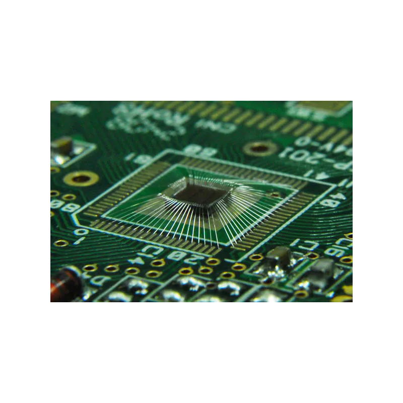
PCB circuit boards -High multilayer circuit board
Details cause analysis: 1. If the circuit board and balance, lifo, prone to PCB bending plate up defects; 2. Into liquid when welding plate tin stove by the liquid surface tension can cause welding arc shaped plate tin thickness is uneven, and because of the hot air blow force and the gravity of the solder tin hang soldersag nozzles, the SMT SMT parts of welding is not easy to stick, easy to cause parts of migration or tablet after welding phenomenon. 3. The smaller tin PCB solder pad surface tin arc shape, the more obvious, flatness, the worse. Solution: less than 14 mil solder for BGA packaging board or plate with relatively high flatness requirement, consider tin exist hidden danger, do not recommend to make tin circuit board, can change to do heavy gold, gold-plated, if the customer must make spray tin circuit board, must clearly customer requirement for flatness.


