


What's the function and principle of PCB via hole?
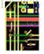
As shown in the figure, what is the function and principle of adding grounding via hole near via hole of the trace?
A: the vias of PCB board can be divided into the following categories according to their functions:
1. Signal vias (via structure requirements have the least impact on signals)
2. Power and ground vias (via structure requires minimum distributed inductance of vias)
3. Heat dissipation vias (via structure requires minimum thermal resistance of vias)
The vias mentioned above belong to grounding type vias. The function of adding grounding via holes near via holes of traces is to provide a shortest return path for signals.
Note: the via of signal layer change is an impedance discontinuity point, from which the return path of signal will be disconnected. In order to reduce the area surrounded by the signal return path, some ground vias must be drilled around the signal via to provide the shortest signal return path and reduce the EMI radiation of the signal. The radiation increases with the increase of signal frequency.
The following are two return diagrams of signals:
Figure 1:
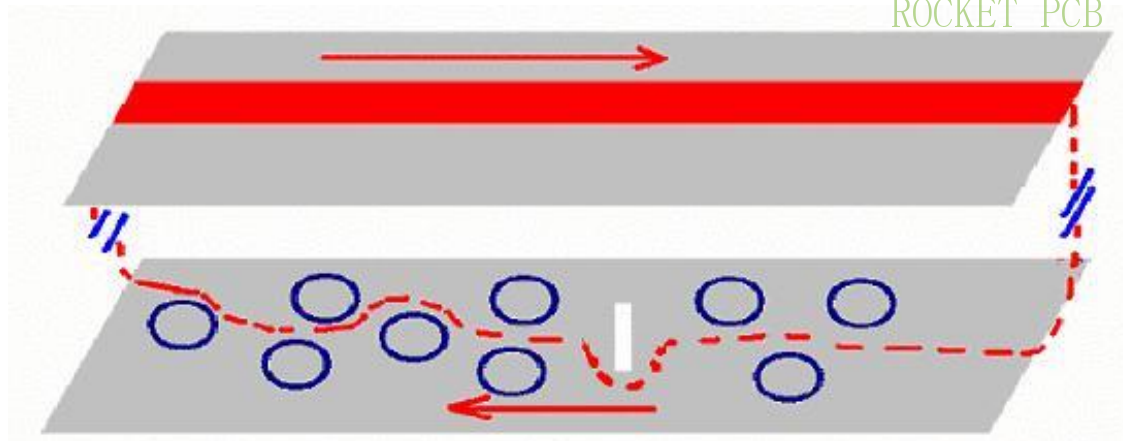
Figure 2
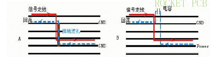
The above question is shown in Figure 2.
Under what circumstances should more ground holes be designed?
There is a saying: more designed via holes will destroy the continuity and integrity of the formation. The effect is counterproductive.
Answer: first of all, if more vias are designed, resulting in the continuity and integrity of the power layer and stratum, this situation should be avoided. These vias will affect the integrity of the power supply, resulting in signal integrity problems, great harm.
For example, the design of ground hole usually occurs in the following three situations:
1. The ground hole is used for heat dissipation;
2. The ground hole is used to connect the ground layer of multi-layer PCB;
3. The location of the via hole used for layer change of high-speed signals
But all these cases should be carried out under the condition of ensuring the integrity of power supply. That is to say, as long as the spacing of ground holes is well controlled, is multi via holes allowed?
Is it OK to arrange via holes at intervals of one fifth of the wavelength?
If I want to ensure the connection of multi-layer boards and lay out more ground holes, although there is no partition, will it affect the integrity of the stratum and power layer?
A: If the copper surface of the power layer and the ground layer is not separated, it will not be affected.
In the current electronic products, the maximum test range of EMI is 1GHz.Then the wavelength of 1GHz signal is 30cm,
The 1 / 4 wavelength of 1GHz signal is 7.5cm = 2952mil. That is to say, if the interval of vias can be less than 2952mil, it can be well connected with the ground and play a good role in shielding. In general, we recommend that every 1000mil grounding via is enough.


