DIY Flexible PCB: A Step-by-Step Guide
If you want to make a flexible PCB at home by yourself, it's not an easy task. Ladies and gentlemen, buckle up and get ready to start learning how to make your own flexible printed circuit boards!
First, you need to design the pattern you want on the software
Second, you need to prepare the materials and tools.
☢ Please note that etching a PCB and removing the toner requires careful handling of chemicals and proper safety measures. If you're attempting this at home, ensure you follow all safety guidelines and use appropriate equipment
1. Design and Preparation :Flex PCB design software
(1) PCB Artist
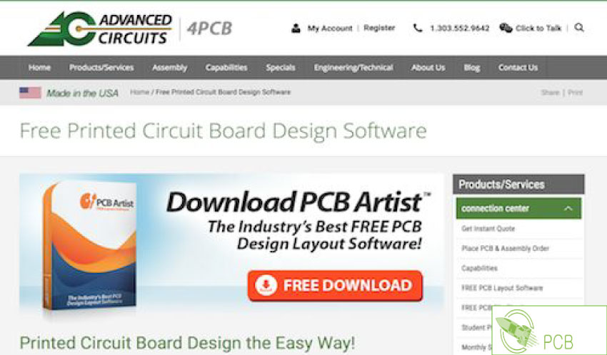
Advanced Circuits is a leading PCB manufacturer with the largest active customer database in the industry. Their developed PCB Artist helps save time and money.
Key Features: Free Gerber file format, component library with over 500,000 parts, integrated schematics, BOM reports in CSV format, DRC error reports between selected projects.
Cost: Free.
(2) Ultiboard
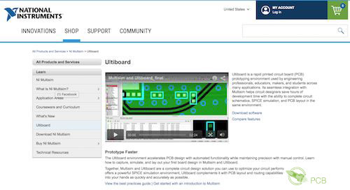
NI leverages its open, software-centric platform, modular hardware, and extensive ecosystem to accelerate engineering success. Electronic engineers specifically choose National Instruments' Ultiboard because it provides a rapid PCB prototyping environment for various applications.
Key Features: Seamless integration with Multisim, completing circuit schematics, SPICE simulation, and PCB layout in the same environment, accelerating PCB design through automatic functions while maintaining precision through manual control, praising Multisim's powerful SPICE simulation environment, featuring PCB layout and routing capabilities.
Cost: Free evaluation; contact for pricing.
(3) Altium Designer 19
Altium is a software company that provides PC-based electronic design software to engineers, offering Designer 17. This PCB design software for electronics engineers is considered the gold standard by many in the industry. Altium Designer 17 is efficient, easy-to-use, and meets the modern needs of professional electronics engineers.
Key Features: Utilizes innovative technologies to help electronic engineers focus less on process and more on design, encouraging more inspired product design by focusing more on the creative aspects of workflow, achieving design automation, endless engineering scope, and very intuitive team collaboration.
Cost: Free trial; contact for pricing.
(4) PCBWeb
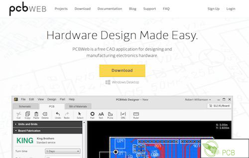
PCBWeb is a fully-featured design tool supporting schematics and PCB layout. For electronic engineers looking to simplify hardware design, PCBWeb is an ideal tool for designing and manufacturing electronic hardware.
Key Features: Use PCBWeb's fast and simple drawing tools to design multi-page schematics, support copper pour and DRC checks, integrate Digi-Key part catalog with BOM manager.
Cost: Free.
(5) BSch3V
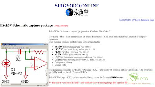
BSch3V is a popular PCB design software tool from Suigyodo Online suitable for engineers needing a free solution. BSch3V is a schematic capture program compatible with Windows Vista/7/8/10, featuring basic functionalities for simplified operations.
Key Features: Basic schematic capture, component library editor, BOM generator, netlist generator, auto-numbering software, CE3 search utility for searching CE3 files, source code and component libraries, Suigyodo also offers the free PCB editor software Minimal Board Editor.
Cost: Free.
Summary: There are many kinds of free PCB design software available, and this list only covers five for reference. When choosing PCB layout software, please conduct background research, checking its specifications, procedures, reliability, certifications, and services offered. This way, you can ensure that the design process for any type of PCB is safe, smooth, and easily accessible.
2. Materials, Material Preparation, and Tools
The most common materials used in flex PCBs include:
· Conductors: Copper foil is the most commonly used material for making flex PCBs due to its excellent conductivity. Thus, a large amount of copper is not needed to make the PCB functional. It can also be provided in fully annealed or low-temperature annealed form, providing better bending characteristics.
· Insulators and Cover Layers: Polyimide film is the most commonly used dielectric and insulator. It can serve as a cover layer, acting as an outer layer to insulate copper conductors.
· PCB Surface Treatment: Prevents copper oxidation and provides a solderable surface. One of the most common surface treatments is Electroless Nickel Immersion Gold (ENIG), which is used on about 80% of circuit boards. This treatment provides a thin, solderable layer of gold, creating a nickel barrier between the copper and the gold wire, thus protecting the copper. Electroless Nickel Electroless Palladium Immersion Gold (ENEPIG) is a three-layer metal coating used on PCBs requiring wire bonding. The electroless nickel protects the copper and prevents contact with other metals. Palladium provides another layer of anti-tarnish protection and a wire bondable surface, preventing nickel corrosion, while the final gold layer increases solderability and acts as an anti-tarnish barrier.
·Copper Etchant: Requires the printed paper to be placed in ferric chloride (copper etchant) for at least 5 minutes for etching.
Tools Used: Solid ink printer
1. Principles of PCB Design Factors to consider before design:
· PCB Layout Concept: All ideas applied to the PCB layout should ultimately be finalized, considering aspects such as circuits and interconnections, dimensions, scope, layout, characteristics, and other features. These considerations provide guidance for the actual manufacturing of the PCB. Correct placement and a sound design concept will help produce the best printed circuit board. It’s important to remember that there are many documents that need to be kept when making a PCB design course. These documents are crucial as they contain the background data and information for each PCB. You can easily trace back and check for errors in the PCB layout; these may be found in the actual schematic diagram or in the actual concept, the materials used, or the component layout. Some layout software has features that allow you to create and automatically save documentation.
Designing a circuit board with any type of software involves different considerations. It is essential to consider the following steps and aspects: To explain the principles of PCB design, one must understand the concept of a PCB as described above—a printed circuit board made of non-conductive substrates (such as glass, fiber, or paper) with copper foil etched to leave conductive areas. The graphical design information necessary to form the circuit on the PCB is the PCB design itself, representing how the circuit will be realized on the PCB. Graphical design information is the first stage of implementing the electronic circuit to achieve the product’s functionality, primarily derived from the description of the product’s purpose.
Without a circuit diagram, nothing can begin. After we create the circuit diagram and install components like ICs and chips, register them in CAD, and input the schematic information into a dedicated PCB layout CAD system, the work is usually handled by specialized layout designers. The circuit designer mainly inputs the necessary information, the minimum required being the PCB size, hole diameters, PCB and copper foil thickness, and the position of installed components, all specified by the circuit designer in advance. The ultimate goal of PCB design is practical application in the form of a PCB, used internally in appliances like air conditioners, refrigerators, TVs, etc. The tools used to materialize the PCB into an electronic circuit board and embed it into the product are dedicated schematic CAD and PCB layout CAD systems. The PCB design process generally includes designing the electronic circuit, converting the circuit into an actual bill of materials (BOM), and then creating a copper foil pattern circuit on the PCB in the form of a pattern representing the circuit and mounted components.
3.DIY Flexible Printed Circuit Steps
① Obtain copper-clad laminate.
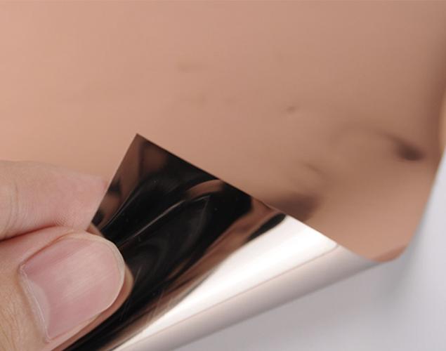
First, prepare some thin polyimide sheets, which have copper on one or both sides. Polyimide is a high-melting yellow polymer, sometimes called Kapton, a common copper coating, and polyimide is DuPont's "Pyralux" material. Pyralux sheets have polyimide thickness, copper thickness, and adhesive thickness ("adhesive" is located between the copper and polyimide, holding everything together). Copper thickness is measured in ounces per square foot, while adhesive and Kapton thickness are measured in mils (1 mil = 0.001 inch). Pyralux LF7062 (as shown) has 1/2 ounce copper, 1/2 mil adhesive, and 1 mil Kapton. This material works fine but is a bit thin for printers and prone to wrinkling. LF9120 contains 1 ounce copper, 1 mil adhesive, and 2 mil Kapton—seems to work best in printers. LF9210 contains 2 ounces copper, 1 mil adhesive, and 1 mil Kapton—harder but works fine. Other options are double-sided copper (Cu/Kapton/Cu laminate held together with adhesive) and rough surfaces, indicated by an "R" at the end of the part number. Rough boards and double-sided boards work fine. However, Pyralux with 2 ounces or thicker copper can be difficult to feed through a printer, especially if both sides are copper. Therefore, the choice of sample is critical. Sometimes Pyralux boards can be bought on eBay. Cut the Pyralux board to 8.5x11 or 8.5x14 inches with scissors or a knife. Avoid getting fingerprints or oil on the copper, as it could block the etching solution later. And to protect the printer, try to keep the edges relatively flat and burr-free.
② Print using a solid ink printer.
If printing directly onto the copper laminate, a solid ink printer is best. They print melted wax, which can provide a protective layer for copper etching, unlike most inkjet printers where the wax adheres well to copper. Unlike laser printers, solid ink printers do not rely on localized charging of the paper surface, which can be problematic when the paper is replaced with a copper sheet. Some models are Tektronix Phaser 840, 850, 860, and Xerox Phaser 8200, 8400, 8500, 8560, and 8860. Most Phaser models are regular laser printers. If a solid ink printer is unavailable, you can use the "toner transfer" method with a laser-printed design instead of this step.
③ Printing on Pyralux.
After drawing the design in a graphics program, manually feed it through the printer and print it in black on the Pyralux sheet. Cyan, magenta, yellow, green (50/50 cyan + yellow), red (50/50 yellow + magenta) seem to work too, but avoid light tones composed of small dots on a white background. The printed area will protect the wax and eventually become the copper traces on the layout.
Note added 3-7-08: Print using "high resolution" or "photo" mode. This setting is typically found in the "print settings" menu of the graphics program. High-resolution mode prints slower, promoting better wax adhesion to the copper. 10 mil (250 micron) wide lines and spaces were printed with a Tektronix Phaser 850 (older model).
In most Phasers, when the copper enters the manual feed and comes out inverted, the copper side is face down. If the manual feed gears cannot catch the paper (more likely with thicker paper), give it a manual push.
④ Etching.
Place the copper-clad laminate in an oscillating etching tank with a mixture of hydrochloric acid and hydrogen peroxide to remove excess copper layers. (This can be done in a basin, shaking by hand, with slightly warmer water to speed up the etching process.) Those with sufficient budget can buy an etching machine online.
The correct ratio of hydrochloric acid and hydrogen peroxide, along with a high-speed oscillating etching tank, is key to achieving quick and perfect etching. After rinsing with water, the etched circuit board can be removed.
⑤ Using acetone or steel wool, remove the black toner, and your PCB board is complete.
Got it? It’s actually pretty simple, For those who know how... Good luck.
4. FAQ
4.1 What is flexible circuit design?
Flexible circuit design refers to the design and layout of printed circuits using flexible substrate materials that can bend, twist, and flex during use.
4.2 Flexible circuits: Design tips and assembly considerations?
That is, the designer must pay attention to certain design aspects:
· Minimum hole sizes.
· Minimum trace widths.
· Minimum spacing between traces and pads.
· Minimum distances to design edges.
· Flex circuit/board outline tolerances.
· Distance of copper geometries from flex circuit/board edges.
· Copper and overall design thicknesses.
4.3 How many layers can a flex PCB have?
The multi-layer capability of flex PCBs allows for highly integrated circuits.
While there is no theoretical limit, practical considerations typically limit flexible PCBs to 12-16 layers or fewer. Higher layers are available, but due to increased complexity, cost, and manufacturing challenges, they are only used for special applications and sometimes require special channel customization.
