Meeting: March 25
Exhibition 2007: March 27-
28 2007 SantaClara Convention and Exhibition Center in Santa Clara, CA www. pcbwest.
Top conferences and exhibitions for Com PCB engineering, design and manufacturing professionals join your industry peers in PCB Design Conference West 2007, you will learn from top speakers in the PCB design industry, inspired by new ideas and technologies, find solutions to your tricky design problems, network with industry promoters and spoilers, and face-to-faceto-
Face your suppliers and suppliers.
Leveraging the input of PCB West alumni, speakers and experts, we bring together experience in PCB design training, networking and technology information collection, which is second to none in the PCB design industry.
From the moment you arrive, until you go home, you will be surrounded by an industry expert trusted by the brain who will not only understand your toughest design issues, but will also show you how
No other meeting offers a targeted experience that you\'ll enjoy in the Pacific West 2007.
If you design or design a PCB or related technology and can only attend a meeting once a year, choose a meeting that really focuses on your personal goals and professional needs: PCB wests7.
You can get quality education there.
The dilemma for each designer is how to be a better and better designer without making expensive design mistakes or technological advances.
At PCB West 2007, we have tailored your meeting plan to suit your needs.
Create your own personalized educational experience by selecting the following courses: * an unparalleled certificate of professional development course consisting of two design excellence courses
Day course and 8 hour courseday tutorials--
All courses are taught by top industry speakers (
View December and tutorial courses on page 67).
* Three diverse and targeted
Daytime technical meeting program for more than 26 short-term courses consisting of two people
Half an hour seminardayseminars (see pages 8-11).
* Free Tuesday program for 14 technical meetings (see page 8-10)
Totally free for all attendees.
Seat first. comefirst-
Service, so arrive early!
* Various registration options including our 5-
Special value passport package (31. 5 hours of in-
If you register before the morning shift, the depth instruction plus the free Tuesday course is only $1,395BirdDeadline).
Where do you get inspiration?
What if your skills and ideas could save the company time and money on future products?
PCB West 2007 full of timesavingand cost-
After attending this year\'s meeting, information on cutting ideas, design and manufacturing strategies, and new technologies that will continue to inspire you.
Where to find a solution
Hundreds of PCB engineering, design and manufacturing professionals participate in PCB West every year to find technical solutions for a variety of projects and problems.
You should be there too. -
In particular, if you specify, recommend or approve the purchase of products and services for your company, or to manufacture them.
You build a network with promoters and promoters in each industry.
The PCB West attendees have been telling us that the network is the top priority.
That\'s why we offer you various opportunities to build networks with industry promoters and promoters ---
Including other meetings and fairs
Only attendees, speakers, exhibitors, industry people, and even the staff of the media group.
Places to meet with suppliers and suppliers. Huge wide-
There may be more exhibitors at a wide variety of trade shows, but it is exhausting to search the floor for the few exhibitors that apply to you.
The display area of PCB West 2007 is only available for our attendees, and in the display area, the size is just right.
PCB West also provides the perfect environment and atmosphere for all important product presentations and supplier meetings, so plan to visit the show now.
We look forward to seeing you in Santa Clara!
Conference ecology-
Chairs on Sunday, March 25
Sponsored by the print circuit design and manufacturing magazine, the top Gun Hall of Fame competition, Monday, March 26. If you have the talent, expertise and knowledge to solve the most challenging PCB design problems, we are
The PCB top gun Hall of Fame competition is held every year in PCB West, aiming to find the world\'s top designers.
During the two-day competition in West, participants will pass a series of tests, including written tests, individual interviews and actual design. The topscorer(s)
In each exhibition, you will enter the Top Gun hall of famepcb and get a plaque and a coveted leather flying jacket from Avirex.
Free admission for all participants-
Technical meetings.
For more information, please visit www. pcbwest. com/topgun.
Sunday, March 25, hosted by the Department of Professional Development for printing circuit design and manufacturing
Participants in the Cypress Room Sunday one o\'clock P. M. professional development certificate course will enjoy a free plated lunch--
Dessert and coffee-
Talk and connect with peers and speakers.
Edit Kathy Najib-
Toth will host a group meeting at the last half of the lunch.
Details will be posted on the website. pcbwest. com.
Monday, March 26 5: 15-sponsored by a printing circuit design and manufacturing wine and cheese mixer
At 6: 15 p. m. all Monday meeting attendees list at Hyatt pool courtyard please attenda special onehour reception with free wine, cheese and othernon-
Alcoholic drinks.
During the wine and cheese mixer, you will learn about your attendees, pick the brains of our speakers, meet with print circuit design and manufacturing personnel, and decompress after a stressful day of class.
On Tuesday, March 21, eight o\'clock A. M-
Eleven o\'clock P. M. in the showroom and other rooms, as noted on Tuesday for free, all attendees, speakers and exhibitors are totally free!
Free Tuesday includes all technical meetings listed on 8-8 pages on Tuesday, March 27
10 of this booklet, the keynote speech described below, the Exhibitor Presentation to be announced later, and the opening night network gala.
Keynote speech 8-
Nine o\'clock A. M. cross current at SCCC theater: where PCB design meets ICs and hardware speakers: mentor Henry Porter, vice president and general manager, system design department, graphics company
The demand for increasingly competitive products is driving the electronics industry, driving advanced
PCB manufacturing technology, using innovative design methods to shorten cycle times and reduce product costs, and expand design team collaboration outside PCB space.
Potts will discuss industry trends such as globalization of MS companies and markets, outsourcing and new manufacturing technologies.
He will cite examples of how the EDA industry has developed new technologies to address these challenges, as well as specific examples of the PCB design field and the future direction of expansion to the ICto-PCBand electro-
Team collaboration in mechanical design.
Henry Potts joined Mentor Graphics in March 1999 as vice president and general manager of system design.
He has more than 33 years of experience in the electronics industry, including inIC and system development experience as president and CEO of aVCfunded startup.
He is senior vice president of HitachiSemiconductor, where he oversees all marketing and product development activities for US microprocessor and embedded productsS.
He also held senior management positions at Motorola, integrated circuit technology, schlenberg and Texas Instruments.
The University of Port holds a bachelor\'s degree in electrical engineering from Southwest Louis Anna State University.
The next day-
Exhibition on the 12 th
Start planning at the showroom at seven o\'clock P. M. so you have plenty of time to attend our 2 day free event
Exhibition of products and services. Cyber Cafe 12-
At 6: 30 p. m. in the showroom, make the most of your visit to the showroom and meet with exhibitors by checking your email
Mail to the conveniently located freeCyber cafe on the exhibition floor.
Opening Night Network event 6-
Happy hour 6-eleven o\'clock P. M.
Enjoy free beer, wine and sodas and delicious food at seven o\'clock P. M. in the showroom network with your peers, speakers and exhibitors.
8-Casino Night
Eleven o\'clock P. M. in the ballroom in Santa Clara, gency viviva in Las Vegas!
Supported by the needs of the public, we once again bring the Las Vegas style action to Santa Clara through our professional casino activities, featuring realistic dice, roulette, 21 pointsNot a gambler? No worries!
You will play with Casino Night \"fun money\" and every dealer will teach you everything you need to know.
This year, you will have the opportunity to win some exciting door awards throughout the evening, and the winner of Texas will hold the \'Em tournament (
Which one is seatedfirst-come, first-serve)
A grand prize will be won.
8-Doug hotel lounge
At eleven o\'clock P. M. , whenever you need to take a break from the exciting Casino Night events, stroll through the Lawrence room in hyattregence to the adjacent Doug mansion lounge for live music and
The infamous portico daos will have a night-long carnival on stage.
If you are a singer or musician, be ready to go to the stage and play with the band.
Wednesday, March 28-
Ten o\'clock A. M-
Do you need to spend some time with your supplier in the showroom at three o\'clock P. M?
Looking for a personal demo of the latest software, products and services?
Then we suggest you plan to visit the exhibition hall on Wednesday (
Since the first day of the exhibition may be busy, it is difficult to give personalized attention). Cyber Cafe 10-
At three o\'clock P. M. in the exhibition hall in the lounge of Doug building, with two 8-
At eleven o\'clock P. M. in the Lawrence room of Hyatt House, don\'t hang out in your room alone!
Join the infamous Porsche for a second night of disruption, dance, networking and tweaking with your long and new industry friends.
There is no food in the lounge so have something to eat before you pass.
However, there will be a well-stocked bar (Including soda)
You bought it. Conference-at-a-
March 25 Sunday eight o\'clock A. M-
Ten o\'clock A. M. registration nine o\'clock A. M-
Professional Development Certificate course at five o\'clock P. M. on December 1--High-Speed Design--
Signal integrity, EMI and crosstalk December 2--
PCR Design 101 T1--
T2-electronic principle and signal integrity-
PCB design for RF applications-
Design RoHS T4--
Design challenges for HDI/
Microvias, including handsOn Design 12-
One o\'clock P. M. Professional Development participants welcome luncheon 12-
Eight o\'clock P. M. PCB strong Lingyun Hall of Fame contest Monday March 26 eight o\'clock A. M.
Four o\'clock P. M. registration nine o\'clock A. M-
Professional Development Certificate course at five o\'clock P. M. on December 1--
Continue from Sunday, December 2--
Continue from nine o\'clock A. M. on Sunday.
010-eleven o\'clock A. M. technical conference course-
Current 011 in PCB trace--Hansd-
Embedded passive design by experienced designers-
Asian manufacturing design 013--
Are you ready to embed resistors and capacitors in your PCRs? 11 am-
1: 30 p. m. lunch break for participants in the technical meeting at twelve o\'clock P. M-
One o\'clock P. M. professional development staff lunch 12-
Eight o\'clock P. M. PCB Hall of Fame 1: 30 p. m-
Five o\'clock P. M. technical meeting course 020--
EMI and crosstalk: Theory, simulation and control 021--Intro to Hands-
Embedded passive design-
Routing seminar 023--
5: 15 flexible circuit design-6:-
Tuesday, March 27, fifteen o\'clock P. M. -eight o\'clock A. M. wine and cheese mixer
Six o\'clock P. M. registration nine o\'clock A. M-
Free Tuesday at eleven o\'clock P. M!
Free for all attendees! 9 am-10 am 030--A Spreadsheet-
Rased-based solutions for capturing today\'s designs 031--
Team collaboration approach for future PCB designer 032--Thermo-
Mechanical advantages of carbon composite laminate embedded in PCB and IC substrates nine o\'clock A. M-
Free course 033 at eleven o\'clock A. M. on Tuesday--Lead-
Free panel: Designer Kit for RoHs and weecompli034--
How to design with Flex at ten o\'clock A. M-
035-free Tuesday at eleven o\'clock A. M. -
Accelerate the secret of NPI 036--
Using an improved traditional PCB manufacturing system 037-innovative process for manufacturing HDI Vias-
Separation of myth and reality in signal integrity 038-
Eleven o\'clock A. M. through Microelectronics-reduce the number of layers
040-free at 12 noon on Tuesday-
High praise-
041-PCB design is limited-
Dealing with new leadsFree World 042--
Love/hate relationship 043-IDF process-
Gigabit snake tube with Maxwell 044--
What is the characteristic impedance? 12-
The exhibition opens at seven o\'clock P. M-
Free exhibitor display five o\'clock P. M.
Eleven o\'clock P. M. opening ceremony party network event, nine o\'clock A. M. on March 28
Eleven o\'clock A. M. technical meeting course 050--
Grounding 051 for noise and EMI control--
RoHS 052-laminated material selection-
Ten questions, ten observations and ten insights to measure PCB manufacturing plant confidence-
A negative news may leave you. -
Ten o\'clock A. M. -Next generation component package-
Three o\'clock P. M. exhibition open morning 10:30-
Free participation from two o\'clock P. M. -1:30
Five o\'clock P. M. technical meeting course 060--
061-RF and
microwave PCB design and basic materials-
Land Pattern creation and RoHS 062--
Basic principle of discrete Fourier transform 063--
Advanced HDI engineering 064--
Design with BGA package 8-
At eleven o\'clock P. M. , the family is resting. It takes two Thursdays, eight o\'clock A. M. on March 29. -
Registration at 2: 30 p. m. nine o\'clock A. M--
Eleven o\'clock A. M. technical meeting course 070--
Vias and its pair of High-
071-high speed digital signal-The IPC-
CAD library standard 072-7351A-
Design high density without sacrificing DFM 073--
Standards and resources at 12: 30 pm
Lunch at 1: 30 p. m-
Five o\'clock P. M. technical meeting course 080--
Practical Guide for signal integrity and board layout 081--The Lead-
Free task and production line 082--
PCB design with flip chip elements 083--
The production process and what the designer needs to know 084--
Lead materialFree, High-Speed and High-
March 30 Friday eight o\'clock A. M-
Ten o\'clock A. M. registration nine o\'clock A. M-
Five o\'clock P. M. certificate of professional development course T5--
Ground abc including analog/digital aircraft--DFM for Lead-
Made free T7--
Placement and wiring of complex pcb T8--
SMT and micro-electronics design principles and leading edge
Development of free assembly process 12-
One o\'clock P. M. Professional Development participants lunch professional development certificate course there are ten courses in this year\'s professional development certificate course-two 2-
Excellent design courses and eight 1-day Tutorials.
These technical courses are taught by industry experts who will provide you with the technical, theoretical, applied and best practice information you need to achieve professional growth and development.
You will receive a certificate of completion for each professional development course you attend and complete.
Note: technical meeting minutes CD-professional development courses are not includedROM. TWO-
December SUN March 25 course and Monday March 26 | nine o\'clock A. M-5 PM IDEC 1--High-Speed Design--
Rick Hartley, L-signal integrity, EMI and crosstalk speakers
3 Communication, avionics system attendees: PCB designers, engineers and managers interested in learning and applying high-tech
Speed concept of electronic products. This two-
The Day course is high-
Speed Design ideas needed to make sure the design is successful with fastand ultra
Fast ICs today and tomorrow.
In today\'s
printed circuit board, the output edge rate is not so much the rate at which the circuit is locked (rise/fall time)
An integrated circuit that causes signal integrity problems, EMI, and crosstalk.
The course will cover parasitic, high
Frequency current, signal to wave propagation, propagation time and speed, signal crosstalk control, power distribution and decoupling, EMI type, EMI source control, EMI coupling control, separation plane and plane Island, PCB layer Stacking, filter and filtration technology, shielding and grounding systems, metal and
Plastic housing, housing slots and conducted EMI filters.
Participants will learn about the cost differences with the manufacturer\'s interface, PCB manufacturing methods and concerns, PCB manufacturing drawings, impedance testing, test coupons and controlled impedance PCB. DEC 2--
PCB Design 101 Speaker: Gary Ferrari, Ferrand Technology Group;
Industry participating in the conference: Enter-
Horizontal PCB designers and others interested in PCB design.
The manager often asks, \"where can I send my entry --
Level designers who learn trade skills?
\"This tutorial is the answer!
Technical meetings at conferences often highlight the latest technologies and techniques, but unfortunately these courses are usually-
The depth of typical novice designers.
The goal of this class is
PCB designers or people who have just started working in this industry.
Attendees will start with the components and schematic to continue the layout and postprocessing.
Attendees will learn how to explain the component spec sheet and schematic, how to plan the component layout, and routing policies, DFM, ft, post-
Deal with and more. ONE-
Sun March 25 | nine o\'clock A. M-5 PM T1--
Speaker of Electronic Principles and signal integrity: UltraCAD attendee Doug Brooks: Is the inductor and capacitor confusing for PCB designers and anyone interested in signal integrity?
Are you not sure what lead inductance means? Why are we worried about bypass capacitors?
This course is for you!
We\'ll start with an overview of resistors, capacitors, inductors, and diodes, and how and why they do these things.
Next, we\'ll look at what happens to the resistance and impedance when we combine these components together in various ways in the circuit.
We will then look at how these principles apply to the main signal integrity issues that motherboard designers face today ---
To prevent ground bounce, EMI, crosstalk, signal reflection and transmission lines, as well as power regulation.
At the end of the course, attendees will learn about the underlying causes of these signal integrity problems, and many of their solutions will become obvious. NEW! T2--
PCB design for RF application speakers: Sychip attendee Andy Kowalewski: any PCB designer who wants a basic understanding of some of the special issues involved in
rf pcb design (RF)applications.
Circuit board is a key element in RF Circuit Design. It has its own special features, which seriously affects the way RF design works. This one-
Day workshop will provide a practical guide to many of the problems faced by modern printed circuit board designers, suitable for qualified circuit board designers facing RF design challenges.
The instructor will introduce some basic RF concepts including wavelength, frequency, Spectrum, modulation, power measurement and capacitance, inductance, resonance and vibration.
Typical components that may be encountered in RF design will be reviewed to discuss their features and the special care required in use.
Issues such as laminate selection, stacking planning, and impedance control will be discussed in depth to understand the problem and its solutions.
The layout and routing strategy will be discussed in detail with reference to the actual circuit and its special requirements in RF application design. NEW! T3--
RoHS speaker design: Gary Ferrari, Ferrand Technology Group;
Doug Sober from KanekaTexas, Jo Wynschenk;
Cookson attendee Rick Love: PCB design and layout engineer, manufacturer, anyone involved in RoHScompliant printed circuit board material selection and final finished product specifications.
This full day workshop will cover the dynamics of material changes and key assembly considerations for designing RoHS compliant pcb.
Industry experts from the entire supply chain will provide information on RoHS\'s basic material considerations, final selection and assembly issues caused by the conversion to lead-free solder paste and wave soldering.
The project includes an introduction to the lead
Free Design for Gary Ferrari.
This overview will inform attendees of the manufacturing and assembly challenges posed by RoHs and lead
Free pcbasseymy.
Doug Sober will cover material selection for RoHS.
One of the most difficult areas for designers and manufacturers is the choice of rohs Compatible materials.
With the increase of the welding temperature and the extension of the contact time, according to the slash sheet, the behavior of the material is not as expected.
This meeting will provide practical guidelines for the selection and identification of laminated materials used in RoHs compliant pcb.
Jo Wynschenk\'s conference on final completion compatibility of RoHs components will provide insights on commonly used final completion and its typical applications based on board type and component details.
Due to compatibility with RoHs components, the final finish will be cut.
Attendees will learn what to expect from a variety of final finishes based on design complexity, material type, board thickness and specific assembly processes.
The workshop will end with Rick Love\'s information about the RoHS Assembly view.
Topics to cover include the impact of lead-free on the assembly process, Assembly Considerations for thick panels and high layers, ways to improve hole filling and reduce old bridging.
A key factor in successful RoHS assembly is following the revised DfA protocol.
The meeting will provide participants with useful design guidelines to help prevent and reduce defects in the assembly process. T4--
Design challenges for HDI/Microvias, including hands
About design speakers: Happy Holden, Mentor Graphics and Mike Fitts, Plexus attendees: PCB engineers, designers, managers and others interested in using HDI/microvias.
The first part of this course will study from ASIC encapsulation, portable products, high
Performance calculation and telecom of dense multi-chip modules.
PCB design rules, materials and selection of PWB structures (
Blind, buried, Micro)
Check and compare.
This tutorial will define buried passive technologies, distributed capacitors, HDI technologies, circuit wiring guides and materials required to allow the use of widely accepted fine features
Spacing and BGAcomponents.
1mm, 0. 8 mm, 0. 65 mm and 0. 5 mm fine-
Pitchcomponents are the focus of pads, spacing, and layer assignments.
Channel routing techniques using blind vias will show how layers can be reduced by 3 times through associated cost reductions.
The examples will be 1,247 and 2,577 I/O 1. 0 mm CCGAs.
Participants were encouraged to raise technical issues for discussion.
The second part of this course is ahands-on session.
It will apply the principles of early learning in the course to reality. world designs.
The second part will begin with a discussion of the CAD toolset, including the use of the actual toolset, to enhance understanding of how HDI can be used to address day-to-day design challenges.
Previous toolset experience is required and must have the ability to work as a team member.
Friday, March 30 | nine o\'clock A. M-5 PM T5--
Ground adc including analog/digital flat speakers: Robert Hanson, Americom workshop attendees: PCB designers, design engineers, and others with knowledge of basic design techniques.
This tutorial will discuss the properties behind grounding.
The concept of high-
The speed current will be analyzed to follow the minimum induction path and how this causes crosstalk in the solid and slotted ground planes.
The following issues and more will be discussed in this tutorial: these should be used for your design--
Single, modified or multi-point?
Can Guard traces really stop the cross talk? Can they resonate?
What causes the nearend and far-
How to measure and simulate the crosstalk?
What is the best way to separate simulations from ECL/PECL and TTL/CMOS?
What are the picketing fences and the 20 hour rule and what can they do to curb emissions?
To minimize radiation and circulating current, how should the shield be connected to the ground?
Why is the loss of the ground plane in the cable causing crosstalk, radiation, reflection, and propagation delays?
Is the potential of the Earth equal?
Why is the best solid ground plane?
What is the intelligent part placement and what is its effect on the ground return current?
Attendees will learn about the concept of moat/floats/suspension bridges, how to lay out split planes--
CMOS/TTL, PECL and analog--
Use the same bias voltage.
The discussion will focus on how to stack the PCB layer (e. g.
Layers 4, 6, 10)
For characteristic impedance and crosstalk control. T6--DFM for Lead-
Free Speaker manufacturing: Gary Ferrari attendees of Ferrand technology group: PCB designer, layout technician and anyone interested in learning DFM technology
Make pcb for free. Lead-
Free Assembly is the latest technological change affecting pcb designers. Cost-
Effective design and manufacture of lead and lead
The free environment constitutes a complete and fundamental component. day session.
The course will be divided into separate interactive discussion groups to study the main issues
Free amine for lead, high performance, HDI and surface finishfreeassembly.
These groups will further explore the challenges posed by hazardous substances directives for the manufacturing and assembly processes.
Finally, the teams will look at new and innovative approaches to test and verify the integrity of the product in terms of lead and leadfree products.
There will be plenty of time to study the individual challenges that attendees face.
Participants should have a clear understanding of the entire DFM issues and their relationship to the RoHs directive. T7--
Placement and wiring of complex pcb speakers: L-Rick Hartley
3. Communication and avionics systems;
Fairfield industry attendee andSusy Webb: PCB designer, design engineer and others looking to understand the concepts behind the placement and routing of complex PCB parts.
Everything you want to know about location and route!
The concept behind parts placement and trajectory routing always seems to be of interest to PCB designers.
The reality is that there are few perfect ways to place parts on a PCB.
Once the parts are placed, there are hundreds of possibilities to route many of the transmission lines of these parts.
Determining which layouts and routing schemes can optimize the design is a physical problem, a suitable problem, and a question of opinion.
This tutorial will focus on the science behind the location and route as well as the opinions of the two mentors.
Attendees will know where to optimize routing, place \"rooms (several views)
, And the impact of the layout on the schematic, EMI, board stack-
Manufacturing, testable, repair and assembly.
It will also cover atypical design processes, routing plans, routing of the best signal integrity, the most important content when routing, the most focused signals, I/O structures, differential pairs, analog pairs
Numbers, etc. T8--
Design Principles and leading edge of SMT and Microehctronic
Speaker for free assembly process development: Vern Solberg attendees: dedicated to the board-
Level design professionals, assembly and testing engineering professionals.
Many new IC device families have more leads and finer contacts than their predecessors, greatly affecting the design and assembly of the circuit board.
In particular, when adjusting the QFP, BGA, and CSP series, board manufacturing tolerances and assembly machine accuracy must be taken into account.
The geometry of the figure is also directly related to the uniformity of process control and welding connections.
The most successful smt procedures are those that implement the process-proven circuit board design rules that specifically define the geometry and spacing of the land pattern of the surface-mounted equipment, affecting manufacturing efficiency,
Maximum assembly process efficiency and yield can only be achieved by properly defining and implementing regulations related to PCB design.
This workshop covers more sophisticated fine processing
4-plate ic with high pitch
Density BGA and fine-pitch chip-
Table BGA device series.
When adjusting these updated, often higher I/O package series, designers and process engineers must recognize discipline, capabilities, and limitations within each other\'s field.
Topics covered include product design principles, lead preparation
Free assembly, fixed pattern and PCB manufacturing and layout guide for SMT and micro electronics.
It also explores the ethics of some alternative packaging and reviews the manufacturer\'s design guidelines and international requirements for lead that meet RoHS and WEEE standards
Free Assembly processing.
Technical meeting 3-
Technical Meeting plan for Monday, March 26 | 9-11 AM 010--
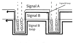
PCB tracking current in speakers: Doug Brooks, UltraCAD attendees: PCB designers and anyone interested in electric flu in PCB tracking.
We hear the definition of \"current is the flow of electrons.
\"But as the drifting speed of the electrons and the flow at the speed of light, there is quite a mess in the flow.
In addition, one would like to know how electrons flow out through a capacitor or space (EMI).
Attendees will learn what \"electronic flow\" means and why this definition (
150 already)is still valid.
As a current stream, how can there be a propagation delay, while the current stays the same anywhere on the trajectory?
Learn how current flows down, terminate, and unterminate along the transmission line, and down along the differential trajectory. NEW! 011--Hands-
Embedded passive design for experienced designer speakers: Mike Fitts, Plexus attendees: experienced designer with previous toolset experience.
How to use high-
Final CAD system for embedded passive parameter design. This hands-
From experience, Mentor Graphics provides a very professional set of tools. The hands-
From experience, each participant will be instructed to use the workstation to complete the design process. (
Depending on the number of people attending the meeting, you may be working in the team. )
This course will provide attendees with the use of an actual toolset to enhance their understanding of how to use buried passive devices to address everyday design challenges.
This is an advanced course. 012--
Design for Asian manufacturing speakers: Happy Holden, directing graphic attendees: PCB designers, design managers, layout technicians, and others interested in the topic.
If you have time to fully understand DFM, then it\'s time to build your motherboard in China!
This workshop will highlight the issues, options, alternatives and conditions that designers need to consider when making printed circuit boards in Asia, especially in China.
Participants will learn how to determine if the manufacturer is able to process the order; how to useIPC-
Select the manufacturer\'s 9151 capability benchmark;
When to control?
Distribution of plating, finish and thickness;
Mechanical Tolerance;
Materials, multi-layer stacking, hole blocking;
Coating, plating problems and why the plating thickness is different; Computing and
2D field solver; and much more. NEW! 013--
Are you ready to embed resistors and capacitors in the pcb?
Speaker: Richard Snogren, Bristlecone LLC attendees: anyone interested in embedded passive devices but not familiar with EP technology. This half-
Day course is a review of the countryof-the-
Embedded passive component material technology for commercial use today.
This course starts with passive component features and performance drivers to embed passive components.
This led to
Conduct in-depth discussions on today\'s commercial materials Group;
Their electrical and physical properties;
Available reasons for choice;
Design, test and trim tools;
And DFM implementation guidelines.
The presentation included discussing the relative cost and cost analysis methods of various technologies.
The course reviews industry initiatives for embedded passive components.
What you will learn: Why and When to embed resistors and capacitors;
Commercial Materials Group;
Design Guidelines and manufacturing processes;
And embedded passive components industry plan.
Monday to March 26 | 1:30-5 PM 020--
EMI and crosstalk: Theory, simulation and control speakers: UltraCAD attendee Doug Brooks: Attendees at this session should have a basic familiarity with PCB design.
Engineers who have not received formal training in crosstalk will find this course useful.
For designers, crosstalk is a noise problem that is difficult to understand and control.
Many engineers use rules of thumb that they really don\'t understand.
This course will first review the cross talk before and after to help attendees understand the resources and differences between the two.
The analysis results will then be used to demonstrate the strengths and weaknesses behind these tools and to help students visualize crosstalk effects.
Finally, some design considerations will be reviewed to show how to eliminate, minimize or even eliminate crosstalk! NEW! 021--Intro to Hands-
About embedded passive design speakers: Happy Holden, directing graphic attendees: PCB designers and others with previous tool experience who are interested in learning how to design embedded to be dynamic.
Participants in this course also participated in the \"013--
Are you ready to embed resistors and capacitors in the pcb?
\"This course is a continuation of the 013 course in many ways.
It will provide attendees with instructions on how to design embedded passive parameters using high-end CAD systems. This hands-
Embedded passive design profiles take advantage of a very professional toolset provided by Mentor Graphics. The hands-
From experience, each participant will be instructed to use the workstation to complete the design process. (
Depending on the number of people attending the meeting, you may be working in the team. )
This will provide attendees with the opportunity to use the actual toolset to enhance their understanding of how buried passive devices can be used to address everyday design challenges. NEW! 022--
Routing workshop speaker: Sychip attendee Andy Kowalewski: PCB designer and anyone with basic knowledge of PCB physical design.
This workshop is for anyone who wants to learn handcraft
Improve their existing routing skills.
This presentation will cover the design sheet
Side assembly with four
Layer structure and multi-layer components with higher layers.
Then there is a detailed layout and routing policy that will show many specific routing examples for discussion.
General placement and routing tips will be covered throughout the presentation and listed at the end for easy review. NEW! 023--
Flexible circuit design Speaker: Joe Fjelstad, silicon tube attendee: PCB designer, IC Packaging specialist, system and hardware engineer and assembly and testing engineer.
Design guidelines are reviewed in this course, including land patterns, viahole layout and cabling, flexible laminated materials (
Polyester, polyester), fabrication (
Metallized and electroplating included)
And assembly, as well as special circumstances that require reinforcement.
It will also introduce the main flex standards.
All Tuesday meetings are free for all conference and exhibition participants.
They\'re not part of 3-
Technical meetings. TUE MAR 27 | 9-10 AM NEW! 030--A Spreadsheet-
Solutions based on capturing today\'s Design speakers: Vikas Kohli, Cadence Design Systems, and Ken Holman, Motorola attendee: Design engineer, manager, R & D engineer, electrical engineer.
It is difficult for designers to use these devices quickly and accurately in schematic diagrams.
Designers of highly restricted motherboards, backboards, and SiPs often see some problems during schematic design capture, including: symbol creation for large pins
Statistical devices, logical function representation with graphical symbols, and limited page editor scope.
In order to avoid these problems, the design engineer uses electronic tables such as Excel to obtain the connection of large equipment.
They have created custom utilities to create physical network lists from spreadsheets to drive the layout.
However, there are problems with this approach that do not support related circuits, lack of connection knowledge, and mechanisms that do not capture constraints.
This article will discuss ways and tools to solve these problems.
The usage model of the new design capture paradigm using spreadsheets will be described.
A case study by Motorola will show the benefits of this approach than traditional schematic-based design capture. NEW! 031--
Team collaboration approach for future polysilicon designer speakers: Cisco attendee Glenn Torrance and Peter Thurburn: PCB designer and design engineer, design team and project manager, and any of
This article will discuss ways to allow the designer team to design at the same time.
Regardless of whether the team is close or not, partitions can achieve access to a single database.
As the market and team environment become more and more important, the role of PCB designers today is changing dramatically.
Case studies and live presentations will be conducted so that each participant has a clear understanding of the benefits of teamwork and the impact of concurrent design engineering. NEW! 032--Thermo-
Mechanical advantages of carbon composite laminate embedded in PCB and IC substrate speakers: ThermalWorks attendees Alex Mangrolia and Kris Vasoya: PCB and IC designers looking for new materials to solve thermal management
Discuss a composite laminate that can handle the heat, CTE, rigidity and weight problems present in the pcb.
This presentation covers the advantages of thermal conductivity, density, tensile elastic modulus and dielectric constant of new materials. TUE MAR 27 | 9-11 AM 033--Lead-
Moderator: Greg Roberts, EMA Design Automation attendees: PCB designer, design manager and other executive and department managers.
Wait until the design cycle is over to ensure RoHS compliance is acceptable for designs currently being produced, but for new designs, the company must consider RoHs compliance at the beginning of the design phase.
The panel agenda will include the impact of RoHS and weee on the design process;
Managing the impact of RoHS and wee on supply chain, PCB design infrastructure and data management;
The actual impact of the directive;
And achieve compliance with electronic and mechanical equipment under coils and electronic equipment-
Is self-declaration
Compliance options?
The aQ & A meeting will be held after the panel discussion and will have the opportunity to meet with each panel member, other experts and attendees. NEW! 034--
Minco product attendees: PCB designers and mechanical or electrical engineers who want to use flexible circuits as a comprehensive interconnect approach.
Flexible circuits are not just electrical interconnect.
Due to the need for flexible circuit bending and bending during and after installation, it becomes a mechanical device just like an electrical device.
Powerful flexible circuit design is much deeper than just connecting the network.
Minor changes in material selection, material stacking, and wiring functions can determine whether a flexible circuit is working for many years or failing in a matter of minutes.
This course will look at the electrical and mechanical properties that must be included in the design and how they will interact.
The course content will include manufacturing and material differences between flex and rigidpcb and how these differences affect the design process.
In addition, how to select the right materials and stacking, process, termination variety and reinforcement options will also be presented.
Participants will also participate in a hands-on
Use the skills acquired during training in design exercises.
TUE March 27 | 10-11 AM NEW! 035--
Secrets for accelerating NPI speakers: Max Clark, Valor computerised system attendees: PCB design and manufacturing professionals including PCB designer/Manager, Engineering Manager, project manager,
PCB manufacturer and
Assembly Design (DfA)
Is the best way to speed up any NPIprocess.
Learn how to quickly discover manufacturing defects and re-discover them easily
Work at the design stage before the product enters the production workshop.
Understand how DfA enables designers to accurately evaluate designs at any stage-
From installation of components to manufacturing output.
DfA provides you with design statistics to help you with your quotation, planning, and resource allocation.
Improved manufacturing process and rights DfA-first-
Time assembly provides hundreds of assembly and test checks to improve the terminal
Product quality and accelerated designto-manufacture.
Reduce NPI downstream costs and manufacture in a virtual prototype environment.
Powerful database of online parts and packaging (VPL)
CAD/CAM provided-
Ready-made physical models of component packages that support all DFM operations.
Part library searches paper or electronic catalogs by providing the following information
Lines with full automatic input, verification and crossover between BOM/AVL and engineering data--
Just press the button. The result--
Analyze and optimize the process before production, correctly simulate and predict the manufacturing, assembly and testing stages of the manufactured products. NEW! 036--
Innovative processes for manufacturing HDI Vias using improved traditional PCB manufacturing systems
Participants: PCB designers, design, manufacturing and packaging engineers, and others interested in HDI.
An important factor in advanced printed circuit boards
Density Interconnect (HDI).
Because of higher demand
Compared to traditional pcb, HDI continues to develop the speed logic and more compact pcb, providing the utilization of finerpitch components and higher wiring density. HDIhave < 75 [micro]
M line and space, 400 [micro]
M capture pad, and150 [micro]m vias.
Innalabs Holdings.
An innovative process has been developed for building HDI vias, which can be easily integrated into any traditional PBC manufacturing system that uses commonly used processed materials, provided that the existing system has sufficient
This process allows implementation (a)
Compared with the traditional
pcb technology, the diameter of the pad is significantly reduced ,(b)
Alignment with the precise adhesive pad at the center of the hole can be achieved without using the alignment system, and the drilling cracks can be automatically adjusted. Double-
Two-sided and multi-layer pcb can be manufactured using this process.
The discussion will be integrated into the existing regular pcb and the results will be given. NEW! 037--
Signal integrity attendees: Electrical Engineers, PCB designers and design engineers interested in solving signal integrity problems in design.
Speaker: Eric bogating of bogating enterprise, introduced the concept of myth and the principle of \"putting people in\" is to separate myth from reality.
The speaker will apply this method to four myths: the electronic speed in the wire is the speed of the signal, the return current in the diff pair is in the second line, the corner should be avoided in the transmission line, and FR-
4 cannot work at GHz speed. 038--
Reduce the number of layers through micro-electronic speakers: Robert Tarzwell and Ken Bell, attendees of Sierra Express: PCB Engineers, Engineering managers, designers and others.
The micro-electronic printing circuit is very small and very fine in order to make your product smaller.
The line width is as thin as 10 microns (1/3 mil)
Vias with only 25 microns (1 mil)
The micro-circuit greatly increases the density of the package and has fewer layers.
With the addition of buried real micro resistors and capacitors, the future density of electronic products will be further reduced tomorrow.
Using rear pad technology, a unique method for making extremely small circuit boards has been invented.
This meeting will discuss the future design possibilities of new micro-circuits (
Flexible and flexible)
Line width, design and use through hole design, multi-layer structure, micro-flexible circuits and new technologies of real buriedrestors.
The advantages of the new micro HDI circuit, including a significant reduction in the number of layers, will be revealed.
A mini-electronic brochure will be distributed to all participants.
On Tuesday, March 27, eleven o\'clock A. M-12 PM NEW! 040--
Highly restricted PCB design speakers for automatic wiring: Greg Horlick, Cadence design system attendee: Design designer, design layout and design engineer using automatic wiring tools during the design process.
In The World of Nationsof-the-art, highly-
Constraints, high
Density design, it may take a long time to design the route.
This is because the automatic wiring technology does not keep up with the technology used in these designs and cannot adhere to the designer\'s intention.
Therefore, the design of simply placing and routing automatically often fails to produce the desired routing results.
In order to route these types of designs efficiently, the designer must start interacting with the routing engine during placement and SI analysis and continue to interact with the routing engine throughout the design cycle ---
It\'s not just manual wiring as it\'s often done today.
To achieve the desired results, guidance needs to be provided to routerso so that it follows not only design constraints, but also good design practices. NEW! 041--
Dealing with new leads
Attendees at Sierra Express: PCB engineer, engineering manager, designer and others.
This meeting will be presented using some real-world examples.
Reliability-
Free printed circuit boards can handle all the needs of our new lead-free world.
Participants will learn about this new technology, which is not only leading
Free, but really indestructible.
It\'s possible to make lead.
Free PCBs can not only be met, but can actually exceed the more demanding requirements of leadfree assembly. A lead-
Free brochures will be distributed to all participants. NEW! 042--
IDF process: Speaker of love/hate relationship: Cisco attendees: PCB designer, PCB manager and others.
Intermediate data format (IDF)
23 and 33 pcbassem data are allowed to be exchanged between MCAD and ECAD systems.
Reliable and efficient processes for accurate placement of key components can prevent errors and reduce board rotation.
Participants will learn the steps to use the IDF process to effectively exchange data between CAD disciplines, as well as the advantages of learning compared to DXF. NEW! 043--
Gigahit Serpentine with Maxwell speakers: Maxwell oph Socha, Maxwell attendees: PCB designers, engineers, technicians and managers.
This paper discusses the simulation of several common differential signal emission androing Technologies (
Maxwell equation)point ofview.
Particularly interested is the insidepair (P and N)matching.
In the bga-type package, there are many techniques used to escape to differential pairs from adjacent and distant pin fields.
In addition, the signal transitions from the loose coupling area to the tight coupling area.
It is common to use this boot area to increase length for tracking formatting purposes, but is it worth the effort?
Participants will understand the various routing techniques and their impact on transmission line properties and signal integrity. NEW! 044--
What is the characteristic impedance?
Speaker: Eric Bogatin from Bogatin enterprise: PCB designer, engineer, technician and manager.
This course introduces the concept of instantaneous impedance and describes an intuitive way of thinking about the characteristic impedance of the transmission line.
It connects geometry with material properties so that you can connect the intuition of the capacitor with the characteristic impedance. WED MAR 28 | 9-11 AM 050--
Ground to control noise and EMI speakers: L-Rick Hartley
3 Communication, avionics system attendees: PCB designers, circuit design engineers and managers interested in learning the appropriate circuit grounding technology.
This new short-term course introduces the concept of high school needs
For normal operation, the speed circuit and the printed circuit design about the ground circuit are designed to minimize noise and EMI.
The course will cover why we call it grounding, many different \"things\" called grounding, circuit parasitic, high
Frequency current, basic transmission line concept, partner plane, successful PCB stacking, grounding that helps eliminate EMI, split
Not Divided (
Advantages and disadvantages of each)
, The island in the ground, the ground in the IC package and the connector, the ground protection trace (
Advantages and disadvantages)
And RF shielding technology. NEW! 051--
Laminated material selection for RoHS speakers: Doug Sober from Kaneka Texas
Attendees: PCB designers and electrical engineers who are interested in understanding the basic material properties and material selection for RoHs manufacturing.
With the arrival of RoHS, one of the most difficult areas for designers is the choice of laminated materials.
In many cases, it is difficult for even PCB manufacturers to choose rolling compatible materials that are both economical and durable
Effective and executed in various assembly situations.
The increase in the welding temperature and contact time of RoHS components has caused problems in the performance of the materials.
In some cases, the behavior of the material does not meet expectations according to the slash table.
This meeting will provide practical guidelines for the selection and identification of laminated materials used in RoHS compliant pcb.
Potential assembly performance and long-term trade-offs for material coordination
Term reliability will be explored. NEW! 052--
Ten questions, ten observations and ten insights to measure PCB manufacturing plant confidence-
A negative factor may leave you with the Speaker: Richard Snogren, bristlecllc attendees: PCB designers, engineers, technicians and managers.
If you are a very good PCB designer but don\'t know much about evaluating PCB manufacturers and are responsible for recommending people who should take this course.
You can sit in the conference room and listen to the sales report.
You can get a guide through the store.
But if you don\'t know what the customer is important to you, you don\'t know what to ask and what to look.
You may not know what you need.
Taking this course, you will feel confident that you can effectively evaluate the PCB manufacturer\'s ability to meet your needs and ensure a positive relationship in the future.
What you will learn: Ten questions that will clarify the key questions you need to know about your future satisfaction;
There are ten things to look for and look for to ensure your future satisfaction;
Top 10 insights on how to ensure a successful future relationship with the manufacturer. NEW! 053--Next-
Generation assembly package speakers: Joe Fjelstad, silicon tube attendees: PCB designers, manufacturers, and assemblers interested in learning about new assembly packages and their impact on design, manufacturing, and assembly
From the DIP and PGA package of 1970s to the rise of QFP of 80 s, to the ball grid array, and finally the chip-
The Post-90 s scale pack, each decade is characterized by the introduction of unique--anduseful--packaging.
What packaging style will the original equipment manufacturer come up with next, and what impact will it have on board-level design and manufacturing?
Wednesday, March 28-5 PM 060--
Speakers: Rick Hartley, L-RF and microwave for each design and base material
3 Communication, avionics system attendees: PCB designers, engineers, technicians and managers. Ultra-
When designing high-frequency simulation applications, high signal integrity and noise control are the key to the implementation of functions.
This workshop is designed to help better understand the \"what\" and \"why\" of the PCB layout and the
PCB material in high-
Frequency analog circuit.
This course will cover impedance and balance, signal wavelength, propagation delay, critical trajectory length, noise, reflection, skin effect, loss tangents, waveguide and other RF transmission lines, as well as micro-strip. stripline vs. co-
Plane waveguide.
Other highlights include PCB stacking for RFcircuits, shielding and shielding, rf pcb base material properties, selection of RF base materials, rf pcb manufacturing, and rf
pcb assembly. NEW! 061--
Guest Speaker: James C.
SMT Plus attendees: CAD designer, librarian, manufacturing engineer.
The world of land patterns can sometimes be very chaotic.
In this meeting, we will explore the needs of the land model and how many models have been created for various packages without affecting the manufacturing needs.
We will discuss the new components.
In addition, it is possible to understand how the land landscape has moved to a small scale over the years.
The list of partial packages to be discussed includes: 0201, 0402, QFN, MLF, QFP, transistors, power elements, LCN, SON, BGA plus, and more.
In the past few years, changes in SMTprocess have led to the elimination of welding lead.
This impact on the land landscape will be a key point for discussion during the conference.
Some old problems such as Tombstone and tin ball appear again.
We will discuss how the land model affects these projects. 062--
Basic principles of BIT speakers: Gary Ferrari, attendees of Ferrand technology group: PCB designers, design managers, layout technicians and others.
The word \"density (Test Design)
Depending on whether you are dealing with the bare printed circuit board, the final assembly, or the circuit board on the spot, it makes a difference.
This course will help you define DfTissues as they relate to design and costs during manufacturing and assembly.
The discussion will focus on manufacturing and assembly issues that affect product design.
These \"snapshots\" will strengthen the discussion and provide you with guidelines for applying IPC standards to your design in order to make it easier to produce effective, correct-the-first-time PCBs. 063--
Senior HDI engineering Speaker: Happy Holden, Mentor Graphic attendee: PCB designer, design and packaging engineer and others interested in HDI.
With more sophisticated spacing devices generally using higher speed logic, the need for advanced pcb is critical ---
Whether packaged as a board or as a MS.
Participants will study from ASIC encapsulation, portable products, high
Performance Computing and telecom-to-dense multi-chip modules.
PCB wiring modeling, design rules, materials and selection of PCB structures (
Blind, buried, Micro)
Will be checked and compared.
For those who are not familiar with the technology, an overview of the HDI technology is particularly useful. NEW! 064--
Sychip attendee Andy Kowalewski: All PCB interconnect designers currently using or planning to use the BGA package.
This presentation will cover floor area construction and layout cabling for BGAs.
Attendees will learn how to calculate the layering requirements of BGAs based on packaging information and design rules.
Participants will also learn about general design issues and pitfalls to avoid, including tips on placement, General wiring, power allocation, and assembly.
A design checklist is included in the presentation for easy review of the material.
This is a must for anyone who wants a low designLow cost-
Coutu pcb with BGAs. THU MAR 29 | 9-11 AM 070--
Vias and its pair of High-
Speed om workshop attendees: PCB designers, design managers and other people who are interested in the special sexy behind vies.
Vias is much more than the hole;
They will have a profound impact on your digital signal.
This course will cover the mechanical properties of vias--
From drilling and plating to lamination, electrolysis and plating.
Participants will learn more about the capacitance and inductance of vias;
Return Current and its relationship with vias; through-
Hole, blind, buried and micro;
Drilling method; aspectratios;
Cost tradeoff.
The discussion will focus on whether vias and autorouters are compatible with HDI, the capacitance and inductance of vias through the problem of discontinuu\' and via resonance (through-
Hole, blind, buried)
, Eliminates the reflection of vias and returns current and intelligence by placing. NEW! 071--The IPC-
7351A CAD library Standard Speaker: Tom Hausherr, PCB Library all PCB designers, CAD clerk, EE engineer, CAD manager and engineering manager who want to extend the basics of PCB layout.
This course is about using ipc-7351.
The materials covered include mathematical modeling of welding joint analysis and tolerance, new component family of IPC7351, newlead-
Free data, BGA layout considerations, and SMT are available through fanout and routing technologies.
The basic elements of IPC are also included
7351: naming convention, Courtyard, 3-
Layer environment, component orientation, I and mode origin, Post
Assemble checkpoints and so on.
Discussion includes transition to metrics.
Participants received aIPC-
7351 LP calculator CD-ROM. NEW! 072--
Design high-density speakers without sacrificing DFM speakers: James C.
SMT Plus attendees: CAD designer, librarian, manufacturing engineer.
The packaging assembly MS, as far as possible, can be manufactured in the commission\'s request to understand the various issues so that the product willrun goes smoothly through manufacturing.
Achieving high density requires working relationships between design and manufacturing.
What helps designers is to know what questions to answer, so that meetings and times spent with the manufacturing industry are meaningful and productive.
In such products, some examples will be provided that, while using very small land patterns, a large number of products with very compact assembly space have been built.
These work hand in hand to achieve very high-density circuit boards that have so far been considered impossible.
Understand what manufacturing problems and problems are and how they affect the design rules you may choose to use.
Some of the topics to be introduced include component tolerances, minimum pitch guidelines, rework issues, minimum fillet trends, IPC standards, plate tolerances, manufacturing tolerances, use of 0402 and 0201 components, and more. 073--
Spokesperson for standards and resources: Susy Webb, Fairfield Industries attendees: PCB designers, design managers and others interested in standards and documentation.
This course provides designers with ideas and resources to use when developing company standards and documentation.
It provides tips for organizing input, output, and inspection procedures;
Naming and saving conventions;
And work with specifications and reference materials.
It will also provide a range of software and websites that may be helpful throughout the design process.
March 29 1:30-5 PM 080--
Practical guide speaker for signal integrity and board layout: Suzy Weber, participant at Fairfield Industries.
PCB designers and layout professionals.
This course introduces the basic concepts of pcb for layout with good signal integrity and EMI control.
We will discuss some basic electronic information. without math)
Why these issues are important for board designers and practical ways to implement them into the pcb.
We will also discuss and illustrate good practices for general circuit board layout, including layout, stacking, plane, wiring, etc to achieve a successful design.
The lesson is a rework of the \"design with your thumb\" lesson with a lot of new illustrations. 081--The Lead-
Freedom of authorization and production line Speaker: Robert Hansen, US seminar attendee: PCB designer, manufacturer and anyone worried about their own leadership
Free PCB assembly.
With the emergence of EU RoHS and WEEE Directives, the pcb industry must address the non-compliance.
The main question legally is: who will catch the violators and what kind of punishment will they face?
On the technical side, what type of failure can you expect on the production line due to printing or components?
What is the recommended soldering PAP formula for reflow and wave?
Participants will learn about the facts of the organization, such
Reliability, quality and aesthetics of temperature return and wave soldering.
The dilemma of tin beard (includingreal-
Case study of world tragedy)
It will also be resolved. NEW! 082--
PCB design speaker with flip chip assembly: Sychip attendee Andy Kowalewski: board designer looking to learn about special issues involved in flip design
This workshop on chip components will provide a practical guide to many of the problems faced by modern pixel designer, at a level suitable for competent designers facing the challenge of designing a compact design.
It will cover key trade-offs related to boards that use flip chips.
Advantages and disadvantages of different types of packaging will be discussed and comparedChip technology.
The known good mold and insufficient fill issues will be covered and the mold re-collision for board installation will be detailed.
The design, assembly and manufacture of the circuit board will be described in detail.
Leadership will also be included-
Free and reliability issues. NEW! 083--
Speaker: Gary Ferrari of Ferrand technology group: anyone who wants to know about the manufacturing process and its limitations on the design of printed circuit boards.
Recommended to all levels.
The design of the printed circuit board has evolved into a complex process that penetrates more into the engineering field.
There is a greater focus on the electrical properties of laminated materials, smaller components and smaller plate conductive geometry.
These factors pose a challenge to the printed circuit board manufacturers to produce produ