Comprehensive Guide to Multilayer Flexible PCB (2025)
In the rapidly evolving electronics industry, the demand for compact, lightweight, and high-performance devices has driven advancements in printed circuit board (PCB) technology. In the 1970s, single and double-layer flexible PCBs were already being used in aerospace and military electronics. However, as the need for miniaturization and higher integration of electronic devices grew, particularly for applications requiring higher circuit density, more complex wiring, and enhanced signal integrity, multilayer flexible PCBs emerged in the 1980s. Initially, these multilayer flexible PCBs were primarily used in military, aerospace, medical, and high-end industrial control equipment. With manufacturing advancements from the 1990s to the early 21st century, the cost of multilayer flexible PCBs decreased, leading to their widespread adoption in consumer electronics, automotive electronics, and wearable devices. For instance, foldable smartphones, smartwatches, and ADAS systems rely on the high density, lightweight, and flexible characteristics of multilayer flexible PCBs. This article will delve into the definition, structure, advantages, applications, and design considerations of multilayer flexible PCBs, providing readers with a comprehensive understanding of this innovative technology.
1. What is Multilayer flex PCB?
(1). Definition of Multilayer Flexible PCBs
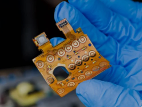
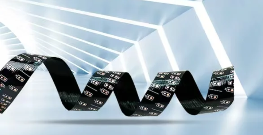
Multilayer flexible PCBs are a type of flexible printed circuit board composed of multiple conductive layers separated by insulating materials. Unlike traditional rigid PCBs, these circuit boards can bend, twist, and fold, making them ideal for applications with stringent space and weight requirements. The layers are interconnected through vias (plated through-holes), enabling complex circuit designs while maintaining a compact form factor.
(2). Materials and Structure
Materials:
The structure of multilayer flexible PCBs consists of a complex arrangement of conductive and insulating layers. The flexible portions of flexible-rigid PCBs are made from flexible PI (polyimide) copper foil materials, falling under the category of multi-flex PCBs. Multi-flex PCBs are a type of traditional flexible-rigid PCBs that have been in use for over three decades. They feature a hybrid structure with rigid substrate materials and flexible substrate materials laminated together, interconnected through plated through-holes that penetrate both rigid and flexible materials. The flexible substrate material typically relies on standard PI copper foil, which is not only applied to the flexible sections but also covers all rigid sections. However, selectively applying PI copper foil to specific sections increases manufacturing complexity, making this approach less common.
When discussing multilayer flexible PCBs, the adhesive used along the Z-axis bonding direction has a relatively high CTE (coefficient of thermal expansion). This can lead to mechanical damage to the plated through-holes during pressure tests or thermal shock tests. Therefore, for PCBs requiring higher thermal reliability, it is essential to avoid using flexible substrate materials and cover layers within the rigid sections, as plated through-holes are typically used in rigid areas.
Additionally, since FR4 prepreg is also a substrate material with a high CTE, the reliability of standard FR4 adhesives and no-flow prepregs must be considered. The Tg (glass transition temperature) of no-flow prepregs for standard FR4 is 105°C, approximately 30°C lower than traditional FR4 prepregs.
Apart from FR4 materials used as rigid substrates, almost any type of rigid material is suitable for multi-flex PCBs, including high-Tg materials, halogen-free materials, and even high-frequency materials.
Most flexible materials used in flexible-rigid PCBs employ PI with or without adhesives, with the latter offering better performance. However, PEN and PET materials can also be used for simple and asymmetrical flexible-rigid circuit board structures. LCP (liquid crystal polymer) materials are considered the best adhesive-free flexible materials, suitable for high-reliability designs and high-speed signal transmission. It is recommended to bake them before application to eliminate moisture absorption issues caused by PI's high hygroscopicity. However, multi-flex PCBs using LCP as the substrate material do not require baking.
In the case of flexible-rigid PCBs, multi-flex circuits can provide multiple flexible layers that can be used simultaneously.
Structure
(1) Conductive Layers
Copper Foil: The primary conductive material, etched to form circuit patterns.
Plated Through-Holes (PTH): Used to connect different layers for electrical conductivity.
(2) Insulating Layers
Polyimide: The most common substrate material, offering excellent thermal stability and flexibility.
Adhesive: Bonds the layers together, ensuring structural integrity.
(3) Coverlay
A protective layer (typically polyimide) used to shield the circuits from environmental factors such as moisture and dust.
(4) Stiffeners
Added to specific areas to provide mechanical support for components or connectors.

2. Applications
Compared to traditional PCBs, multilayer flexible PCBs offer numerous advantages and are widely used across various industries:
(1) Consumer Electronics:
Smartphones: Used to connect displays, cameras, and other components.
Smartwatches, AI Glasses, and Fitness Trackers: Enable compact and flexible designs.
(2) Automotive Electronics:
Engine Control Units (ECUs): Capable of withstanding high temperatures and vibrations.
Infotainment Systems: Provide compact and reliable connections in dashboard systems.
(3) Medical Industry:
Implantable Devices: Used in pacemakers and hearing aids due to their biocompatibility and reliability.
Diagnostic Equipment: Ensure precise signal transmission in MRI and ultrasound devices.
(4) Aerospace and Defense:
Satellites: Lightweight and durable, suitable for space applications.
Military Equipment: Used in communication systems and radar equipment.
3. Advantages of Multilayer Flexible PCB
3.1 Space Efficiency
Ability to bend and fold, enabling three-dimensional packaging and saving space in compact devices like smartphones and wearables.
3.2 High Reliability
Eliminates the need for connectors and solder joints, reducing the risk of failure and excelling in high-stress environments.
3.3 Improved Signal Integrity
Multilayer design supports better signal routing, reducing electromagnetic interference (EMI) and crosstalk.
3.4 Lightweight and Thin Profile
Ideal for applications with strict weight and thickness requirements, such as aerospace and medical devices.
3.5 Reduced Assembly Costs
Minimizes the need for additional connectors and wiring, thereby lowering assembly costs.
4. Design Considerations for Multilayer Flexible PCB
When designing multilayer flexible PCBs, careful attention must be paid to mechanical, electrical, and thermal management factors to ensure optimal performance.
4.1 Bend Radius
The minimum bend radius must be calculated to prevent circuit damage. For example, the formula for the minimum bend radius of a single-sided flexible circuit is:
R=C/2((100-EB )/EB)−D
Where:
R is the bend radius,
C is the copper layer thickness,
D is the dielectric layer thickness,
EBis the elongation percentage of the copper.
4.2 Layer Stackup
A proper layer stackup is critical for signal integrity and thermal management. Signal layers should be placed close to ground layers to minimize electromagnetic interference (EMI).
4.3 Thermal Management
While polyimide materials offer excellent heat dissipation, additional thermal vias or heat sinks may be required for high-power applications.
4.4 Component Placement
Components should be placed away from bending areas to avoid mechanical stress. Stiffeners can be used to support heavy components.
4.5 Compliance with Standards
Designs must adhere to industry standards, such as IPC-2223B, which provides guidelines for flexible circuit design.
5. Challenges and Limitations
Despite their numerous advantages, multilayer flexible PCBs also present certain challenges:
5.1 Higher Costs
Materials and manufacturing processes are more expensive compared to rigid PCBs.
5.2 Manufacturing Complexity
Specialized equipment and techniques are required, increasing production time and costs.
5.3 Limited Current-Carrying Capacity
Due to thinner copper layers, they are less suitable for high-current applications.
6. Future Trends
As technology advances, the application of multilayer flexible PCBs in the electronics field will continue to expand. Key trends include:
6.1 Integration of Rigid-Flex PCBs
Combining the advantages of rigid and flexible PCBs to enable more complex designs.
6.2 Applications in 5G and IoT
Supporting high-speed data transmission and compact designs for next-generation devices.
6.3 Development of Advanced Materials
Creating new materials with improved thermal and electrical properties to enhance performance.
7. Multilayer flexible PCB creates more possibilities for the future
Multilayer flexible PCBs represent a significant advancement in PCB technology, offering unparalleled flexibility, reliability, and performance. Their applications span from consumer electronics to aerospace, and their use continues to grow. Although challenges such as cost and manufacturing complexity exist, ongoing innovation is expected to overcome these limitations, paving the way for more groundbreaking applications in the future. For engineers and designers, understanding the intricacies of multilayer flexible PCBs is crucial to fully leveraging their potential in modern electronics.
By harnessing the unique properties of multilayer flexible PCBs, industries can continue to push the boundaries of electronic design and functionality, unlocking new possibilities.

FAQ:
1. How many layers can a flex PCB have?
A:According to design requirements, flexible printed circuit boards (flex PCBs) can have any number of layers, ranging from a single layer to multiple layers. The breakdown is as follows:
· Single-layer flex PCB – Contains a single conductive layer on a flexible dielectric film.
· Double-layer flex PCB – Consists of two conductive layers separated by a dielectric layer, with electrical connections made through vias.
· Multi-layer flex PCB – Comprises three or more conductive layers, with dielectric insulation layers in between. These are used for complex circuits requiring high density and intricate routing.
2. What is the difference between Flex PCB and FPC?
Flex PCB (Flexible Printed Circuit Board) and FPC (Flexible Printed Circuit) are terms often used interchangeably, but they can have nuanced differences depending on context. Here's a breakdown:
(1)Flex PCB (Flexible Printed Circuit Board):
Definition: Flex PCB refers to a type of printed circuit board that is designed to be flexible, allowing it to bend, fold, or twist to fit into compact or irregularly shaped spaces.
Construction: It typically consists of a thin, flexible substrate (such as polyimide) with conductive traces printed or etched onto it. It may also include additional layers for insulation, shielding, or reinforcement.
Applications: Flex PCBs are used in applications where space and weight savings are critical, such as in consumer electronics (e.g., smartphones, wearables), medical devices, automotive systems, and aerospace technology.
(2). FPC (Flexible Printed Circuit):
Definition: FPC is essentially the same as Flex PCB, but the term is often used more broadly to describe any flexible circuit, including simpler designs like single-layer circuits or connectors.
Construction: FPCs can range from very simple single-layer circuits to more complex multi-layer designs. They are made using similar materials as Flex PCBs, such as polyimide or polyester films.
Applications: FPCs are used in a wide variety of applications, including flexible connectors, ribbon cables, and simple circuits in devices like printers, cameras, and LCD displays.
Key Differences:
Scope: Flex PCB is often used to describe more complex, multi-layer flexible circuits, while FPC can refer to both simple and complex flexible circuits.
Usage: Flex PCB is more commonly used in technical or engineering contexts, whereas FPC might be used more broadly in manufacturing or general discussions.
Complexity: Flex PCBs are typically associated with more advanced designs, including multi-layer circuits with additional features like stiffeners or shielding, while FPCs might refer to simpler, single-layer designs.
In practice, the terms are often used interchangeably, and the distinction between them can vary depending on the industry or specific application. Both refer to flexible circuits designed to provide electrical connections in environments where traditional rigid PCB are not suitable.
3. What is the difference between PCB and PWB?
The terms PCB (Printed Circuit Board) and PWB (Printed Wiring Board) are closely related but have different meanings:
PCB (Printed Circuit Board):
A broader, more modern term that refers to a circuit board that has both conductive pathways and electronic components.
Used in a variety of applications, including rigid, flexible, and rigid-flex circuits.
PCBs can be single-layer, dual-layer, or multi-layer, and may include advanced features such as embedded components.
PWB (Printed Wiring Board):
This is an older term that was primarily used before PCBs became commonplace.
Refers to a circuit board with only conductive traces, but no mounted electronic components.
Once components are added, the PWB becomes a PCB.
Main differences:
PCBs include both conductive traces and mounted electronic components.
PWB refers only to the bare board with traces but no components.
Today, PCB is the standard term, while PWB is rarely used.


