High-end HDI anylayer mass production capacity-Rocket PCB
Electronic industry enters 5G Era, HDI PCB ushered in any layer of interconnection and fine wiring needs
HDI (high density interconnect) PCB is widely used in smart phones, tablet computers and high-end consumer electronic products. Since the 1990s, HDI has developed for many years and experienced several changes. The early technology originated in Japan. Based on the subtraction method or printing and etching process, it relies on micro through holes to realize the characteristics of high-density interconnect.
With the further development of 5G, smart phones, tablet computers, wearable devices and other electronic products tend to be more intelligent, miniaturized, high-frequency, high-speed and highly integrated, and the components to be carried on PCB are also increasing significantly. At the same time, with the improvement of 5G intelligent products' high frequency, high-speed transmission and functions, the requirements for the screen are getting larger and larger, the resolution is getting higher and higher, and the power consumption has become the key point. At present, there is no new technology breakthrough in the battery part, only the space of the main board of the mobile phone can be continuously compressed, and the size, total amount and volume of the main board of the mobile phone are constantly shrinking.
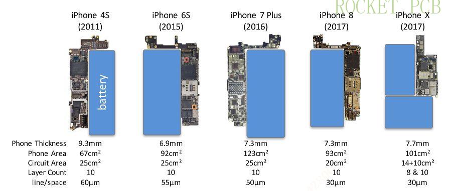
Evolution of smart phones
(source: ifixit, techinsightsTeardown. com、HIS、Prismark Partners)
When the high integration and PCB space cannot be increased, the PCB wiring becomes more intensive, the wire width and spacing are reduced, the distance between the hole diameter and the center is reduced, and the thickness of the insulation layer is reduced. Therefore, the anylayer interconnection structure with more stacking layers, smaller line spacing and more functional modules + SLP Substrate-like PCB board technology (MSAP) becomes the best solution. The capacity of traditional HDI process is limited, which is difficult to meet.
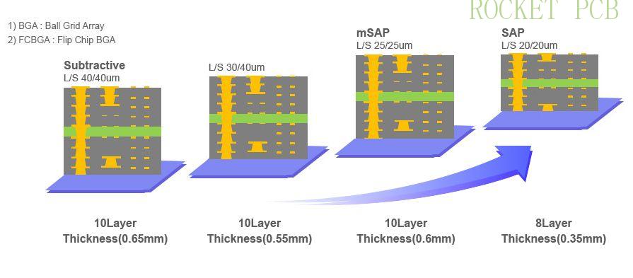
The trend of high-end HDI board
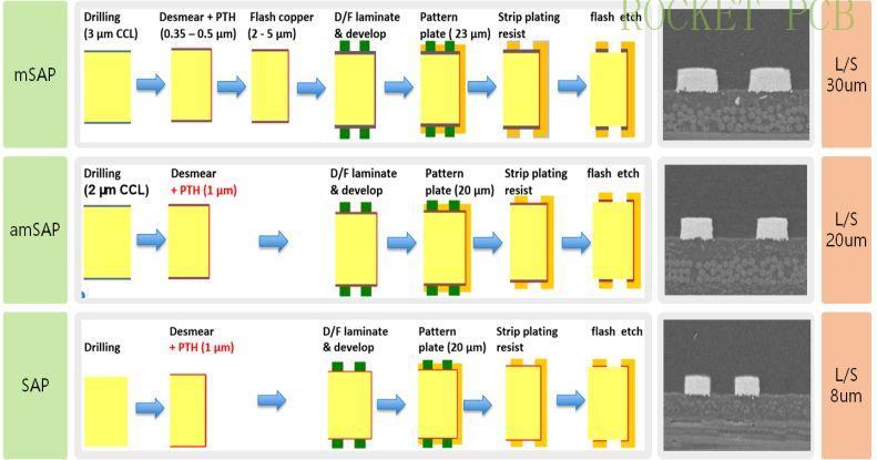
Introduction to MSAP, amsap and SAP processes
The technology development of smart phones is dominated by apple. Since the iPhone 4, HDI anylayer interconnection technology has been used, and the iPhone 8 has been using the SLP (Substrate-like PCB) technology (MSAP). The Galaxy series released by Samsung 2019 also uses the SLP technology. Since 2018, Huawei, oppo, vivo and Xiaomi flagship mobile phones have been equipped with HDI anylayer interconnection technology. In 2019, Huawei launched P30 Pro 5G, vivo iqoo 5G and oppo Reno 5G in the domestic market, all of which adopt HDI anylayer interconnection + main board sandwich structure,. It is estimated that Huawei will introduce SLP like carrier technology in its flagship in 2020, which will be adopted by global mobile phone manufacturers in the future.

Smart phone disassembly diagram (stacked sandwich structure)
Technology enabling development
HDI anylayer interconnection is a high-density connection technology, which has a high technical threshold. The main processing difficulties are layer alignment, laser drilling, hole filling electroplating, dense circuit processing, etc. Among them, Victory Giant technology has built the industry top equipment and well-known materials for benchmarking industry. At present, the domestic PCB manufacturers with high process capability and large production capacity mainly include founder, Victory Giant technology and Shantou Goworld, etc.
The requirements for PCB factory about high-end any layer HDI & any layer PCB technology
1. Equipment, raw materials, liquid medicine:
·Equipment: Laminating machine, laser five generation drilling machine, VCP hole filling, full process DI equipment, vacuum etching and other high-end mainstream equipment in the industry.
·Raw materials: the industry high-end HDI mainstream material manufacturers, including Taiwan, domestic, Japanese, etc.
·Liquid medicine: the mainstream liquid medicine system of Germany and Japan.
·
2. Process capability:
·Fine line capacity: mass production 40 / 40um, R & D 35 / 35um;
·Alignment ability: 14L any layer interconnection, laser micropore D + 5MIL;
·Thin core board capacity: 50um thin core capacity; 1027 / 1017 PP layer adding capacity; 10L any layer interconnection product, board thickness 0,55mm capacity;
·Laser aperture: conventional min 50um, any layer interconnection x-via min 50um;
· BGA Pitch:0. 35mm;
·At this stage, it has the mass production capacity of HDI 14L anylayer (interconnection of any layer)..
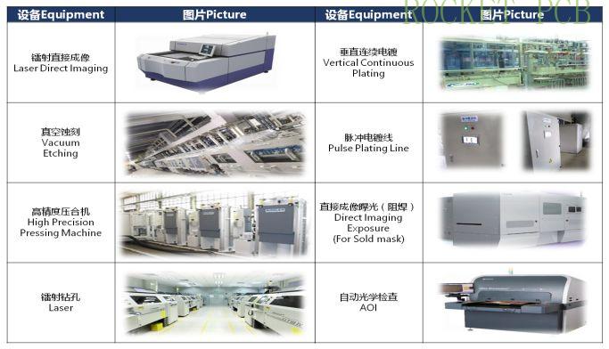
Major equipment
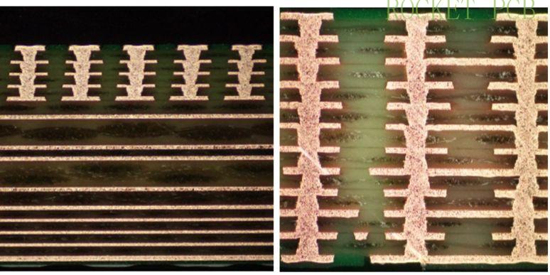
Metallographic of any layer HDI product
3. Processing example:
A number of 10l-14l HDI anylayer (any interconnection structure) samples have been proofed successively, involving the application fields of smart phones, high-end tablets, smart watches and other products.
High technology, high quality, high quality service
Focus on 5G consumer 3C products
With the boom of PCB industry and the accelerated transfer of production capacity to the mainland of China, the industry boom continues to grow. PCB accounted for a rapid increase in mainland China, rising from 14% in 2011 to 23% in 2018. Meanwhile, the domestic PCB plant is actively launching the established HDI plant in 2019 to expand the high level HDI capacity (ounder, Suntak,King Wong, oskang, etc. ), because the HDI production line has heavy investment, relatively high technical requirements, and electroplating production lines, etc. , with the environmental approval threshold, which is the barriers to entry of HDI production line, especially the expansion of high-level HDI production line, need to be prepared 1-2 years in advance, so it is impossible to form large-scale new capacity and release it in a short time.
In the process of accelerating global PCB capacity transfer to mainland China, Victory Giant technology,Shennan circuit are the outstanding representative. In the period of serious shortage of HDI high-level PCB capacity in 5G era, the layout and capacity preparation of high-level HDI anylayer (any layer interconnection structure) should be carried out one year in advance, it is expected that in Q3 2020, SLP products will be put into production with 35000m2 / month production capacity (MSAP process).
The newly built smart factory has a high level of automation, ranking the world leading position, and its per capita efficiency and profit level continue to improve. Relying on industry 4. 0 intelligent factory and industrial automation production system, it has high efficiency, good quality, short delivery time, large production capacity and low cost.
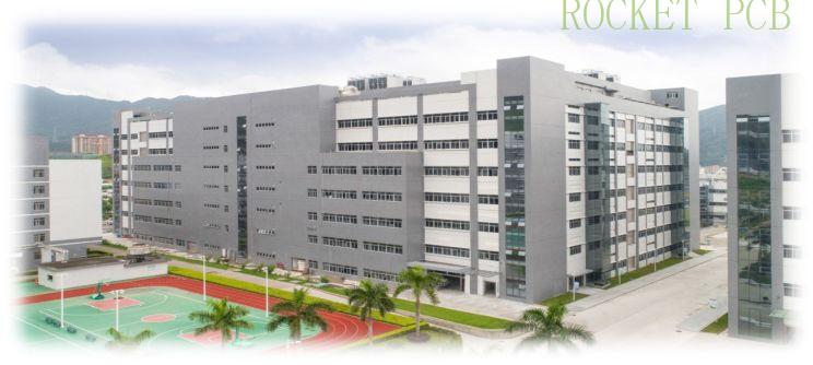
HDI plant
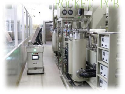
Intelligent production line
In terms of talents, a group of technical, manufacturing, quality and sales talents with many years of high-level HDI production and management experience have been introduced from large factories in Europe, America and Taiwan. A professional team has been formed, and a perfect management system and quality system have been established. Implemented batch control and improved quality traceability system, and established SPC control (Thick distribution, linewidth, impedance, …). All staff should establish quality awareness (no manufacturing, no acceptance, no outflow), market-oriented, customer-centered, improve product quality, improve after-sales service, and continuously improve customer satisfaction.
Rocket PCB has a unique resource advantage of PCB manufacturers in the field of high-level HDI, helping high-tech enterprise users to solve the production problems of high-level HDI. You only need to send your gerber requirements, we will serve you wholeheartedly at the first time, and guarantee the quality and delivery time of PCB board in the whole PCB process. We always adhere to the customer first orientation.


