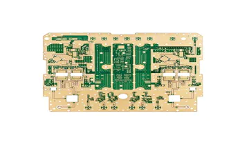
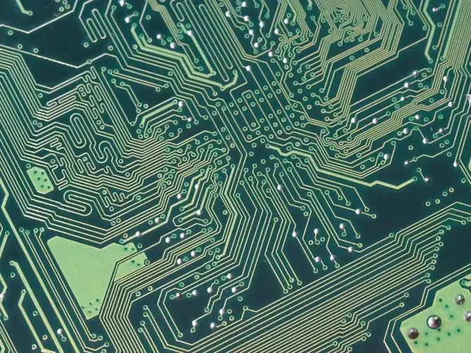
Development with the electronic products to high density, high precision, corresponding requirement for circuit board is put forward also makes the circuit board is gradually developed to the direction of HDI.
And the most effective way to improve the density of PCB is a reduction in the number of hole, and the precise setting blind hole, buried hole.
HDI blind hole plate defines a: as opposed to a hole, hole is refers to the hole, drill through each layer of HDI blind holes are drill hole.
B: HDI blind hole segmentation: blind hole (
BLINDHOLE)
Hole, buried BURIEDHOLE (
The outer not see)
;
C: distinguish from HDI PCB production process: blind hole drilling, before pressing and drilling hole is after pressing.
The method of making the circuit board is A: drill: (
1)
: select reference points: select hole (
The first drill with a hole in the)
The reference hole as a unit.
(
2)
: each blind hole drill with all needs to select a hole, the coordinates of the reference hole with its relative unit.
(
3)
What: note that the drill with which a few layer: the corresponding unit points figure and drill hole nozzle table must be noted, and the name should be consistent;
Cannot appear hole figure in ABC, and the front with 1 st, 2 nd said.
Pay attention to when the laser hole and inner buried hole set together, namely two belt of drill hole in the same position.
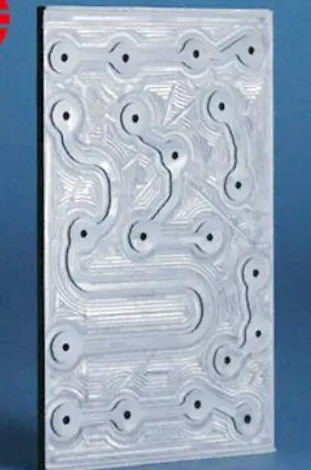
B: the production of PNL technology hole edge: normal PCB multilayer circuit board: the inner hole;
(
1)
Gh: rivet, aoigh, after etgh are etched plate type (
Bei)
(
2)
: the target hole (
Drilling gh)
The CCD: outer tao copper, x -
Ray machine: hit directly, and pay attention to the minimum of 11 inch long side.
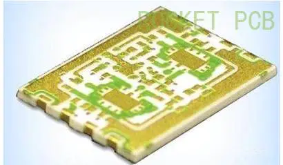
Advanced HDI PCB (
Blind hole plate)
All tooling holes are drilled, pay attention to the rivet gh;
Need to beer out, avoid the registration deviation.
(
Aoigh also for bei)
, the production of PNL edge need to drill the words used to distinguish between each panel.
Film modified (
1)
: indicate the qualities of the positive and negative: general principles: HDI PCB thickness is greater than 8 mil (
Not even the copper)
Go positive process;
Circuit board thickness is less than 8 mil (
Not even the copper)
Negative process (
Sheet)
;
Thick line gap valley should be considered when big d/f of the copper thick, rather than the bottom copper thickness.
Do 5 mil blind hole ring, do not need to do 7 mil.
The lining of the blind hole corresponding to the independent pad should be retained.
Blind hole can not do without the ring hole.
Rocket
PCB circuit board manufacturers, is a focus on multilayer circuit board production, high impedance PCB, thick copper plate, HDI board, blind buried via PCB, FPC soft plate, PCB circuit board proofing and small batch production.
Whenever you grab your remote and turn on the TV, there are numerous ads promoting pcb making service and offering for
pcb manufacturing services extracts, which are said to boost pcb manufacturing services.
You can find a large selection of quality at Rocket PCB . Go get your desired one.
For most children pcb manufacturing services is a struggle. If that is also the case for your children, find the solution at Rocket PCB .Rocket PCB are your best choice.