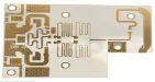
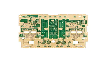
Application examples of semi rigid flex PCB in mobile phones
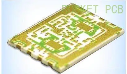
Application examples of semi rigid flex PCB in mobile phones


Quick Links
About Us
Contact Us
Tel:(+86) 158 9965 5195
Office:(+86) 755 23040566
E-mail:sales@sllpcb.com
Microsoft Teams:hank_168
WhatsApp:+86 186 0723 3179
Office Address:2207,Bid 4,He Gu Shan Hui Cheng,35#,Guang Tian Ro Yanluo street, Song Gang Town,518105 SHENZHEN, CHINA
Plant ADD: No 69, Lianfeng North Road, Xianxi Area, ChangAn Town, Dongguan, China.