PRODUCTS
The five considerations of PCB circuit board puzzle design
by:Rocket PCB
2020-07-23
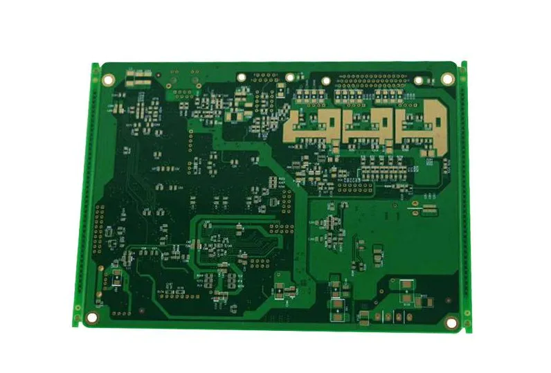
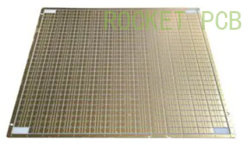
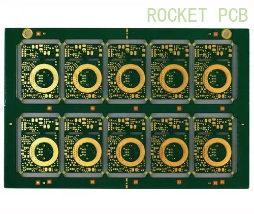
Because each industry products are different, so the application of PCB circuit board size also is different, some of the electronics industry of PCB circuit board is smaller, often designed to puzzle the way, can not only facilitate the processing production of electronics factory, also can reduce waste, reduce the cost.
In order to facilitate PCB manufacturing and PCBA processing, puzzle in PCB design, a lot of problems need to pay attention to.
Puzzle HDI circuit board PCB design considerations to facilitate production, usually need to design PCB circuit board puzzle Mark point, V groove, technological edge.
A, PCB proofing puzzle shape 1.
PCB proofing puzzle frame (
Clamping side)
Closed loop design, should be adopted to ensure the PCB after makeup on the fixture will not deformation.
2.
PCB proofing puzzle width of 260 mm or less (
SIEMENS line)
Or 300 mm or less (
FUJI line)
;
If you need automatic dispensing, PCB makeup width x length is 125 mm * 180 mm or less.
3.
Makeup;
But don't Mosaic board of Yin and Yang;
2, 1 V groove.
After open the V groove, the thickness of the remaining X should be (
1/4 ~ 1/3)
Thickness L, X must be zero or minimum thickness.
4mm。
For bearing heavy board recommended limit, for bearing a lighter board recommended limit.
2.
Dislocation S V groove on both sides of the up and down incision should be less than 0.
1毫米;
Because of the limitation of the minimum thickness of effective thickness less than 1.
2 mm plate, unfavorable used V groove makeup.
Three, Mark the point 1.
Set the benchmark anchor point, usually around the anchor point set aside is bigger than the 1.
5 mm in welding area.
2.
Help for SMT machine optical positioning have SMT components of PCB diagonal has at least two asymmetric benchmark, the whole piece of PCB optical orientation with reference point in the whole piece of PCB diagonal corresponding position;
Block PCB optical orientation with reference point is in commonly block PCB circuit board is diagonal position accordingly.
3.
For the lead spacing 0 or less.
5 mm QFP (
Square flat pack)
And the ball distance between 0 or less.
8 mm BGA (
Ball grid array package)
Device, in order to improve the SMT precision, requires two diagonal set the benchmark in the IC.
Four, the craft is 1.
Makeup frame and small plate, plate and small plate near the connection point between cannot have big device or out of the device, with the edge of the PCB circuit boards and components should be greater than zero.
The space of 5 mm, in order to ensure the normal operation of the cutting tool.
Five, the plate positioning hole 1.
65 mm of QFP should be set in the diagonal location;
Used to puzzle PCB plate locating datum symbol should be used in pairs, decorated in diagonal positioning elements.
2.
Large components should have positioning column or positioning hole, such as I/O interface, microphone, battery interface, micro switch, headphone jack, motor, etc.
A good PCB designers, in the idea of design, want to consider the factors of production, convenient processing, improve the production efficiency, reduce production cost.
Rocket PCB Solution Ltd. will continue to build a corporate culture that respects and values the unique strengths and cultural differences of our associates, customers and community.
To live healthy, you need to eat healthy; to eat healthy, you need to think healthy; to think healthy, you need to read health; to read healthy, you need to follow Rocket PCB .
Rocket PCB Solution Ltd. deems pcb making service as evolutionary rather than revolutionary. We've always had these 'social commerce' marketplaces in some form.
Custom message


