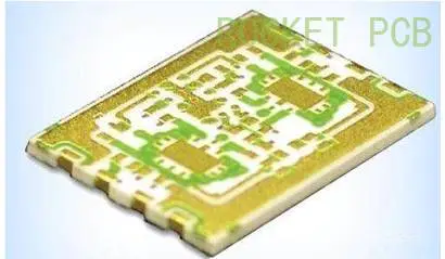
Copper is an important link in PCB circuit board design, so-called copper clad, is to spare space on PCB as datum, filled with a solid copper, the copper copper area is known as irrigation.
The meaning of the copper clad is, reducing ground impedance, improve the anti-interference ability;
Lower pressure drop, and improve the power efficiency;
Connected to the ground, but also can reduce the loop area.
Also out to keep as much as possible when PCB welding deformation, the purpose of most of the PCB manufacturer will ask empty expanse of PCB PCB designer on PCB who or the ground grid.
As everybody knows, under the condition of high frequency, wiring of distributed capacitance on the
printed circuit board will work, when the length is more than 1/20 of noise frequency corresponding wavelength, can produce the antenna effect, the noise will launch out through wiring.
If there are bad grounding copper clad in PCB, copper clad became the tool of transmission noise.
In the high frequency circuit, therefore, don't think that somewhere in the ground after the, this is the 'ground'.
Must to less than the spacing of lambda / 20, punch a hole in the cabling, and multilayer ground plane 'well grounded'.
If the copper clad processing properly, copper clad with increasing electric current, not only has played a dual role of shielding interference.
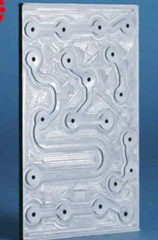
Copper clad generally there are two basic ways, is a large area of copper and copper grid.
Often asked, large area of copper clad copper or grid good.
It is bad to generalize!
Large copper clad, with the increasing current and double shielding, but large copper clad, if a wave soldering, the board may become warped up, even bubbles.
So large copper clad, general will also open a few slots, alleviate blister copper foil.
WeChat public number: dongguan LED chamber of commerce in pure copper mesh is main or shielding effect, increase the current function is reduced, from the perspective of heat dissipation, the grid is good,
It reduces the heating surface of copper)
And have played an important role in certain electromagnetic shielding.
Blind buried orifice (
Printed circuit board)
PCB PCB but it should be pointed out that, the grid is made by alternating direction of running, we know for circuit, line width for the work frequency of the circuit board has its corresponding 'electrical length' (
Computed by dividing the actual size of the working frequency of the corresponding digital frequency, concrete books)
, when the working frequency is not high, may be the role of the grid lines is not obvious, once the electrical length and working frequency matching, very bad, you will find that the circuit won't work properly, emission signal interference system work everywhere.
So for using copper mesh colleagues, my suggestion is that according to the design of the circuit board work situation.
As a result, the high frequency circuit against interference demanding multi-purpose copper grid, low frequency circuit with high current circuits commonly used full copper.
So we in the copper clad copper in order to make our desired effect, then copper clad problems which need to be paid attention to: 1, if the PCB is more, there are SGND, AGND and GND, is depending on the position of PCB board face, respectively to the main 'to' independent copper clad as reference point, to digital and analog to separate copper clad.
At the same time before the copper clad, first bold corresponding power cords: 5.
0V、3.
3 v, etc.
Thus, have formed the different shape of deformation structure.
2, to different single point of connection, it is through 0 o resistance or magnetic beads or inductance connection.
The middle tier 3, PCB PCB wiring empty area don't copper clad.
Because you are more difficult to do make the copper clad 'well grounded'.
4, a lonely island,
Dead zones)
Problem, if it is big, then define a pass hole added to also do not cost much.
5, equipment internal metal, such as metal heat sink, metal reinforcing bar, etc. , must achieve 'well grounded'.
6, three-terminal voltage regulator of metal heat dissipation, must be well grounded.
Crystals near ground isolation belt, must be well grounded.
7, the copper clad near the crystals.
Crystals is a high frequency emission sources in the circuit, it is around copper crystals, then crystal vibration of the shell shall be grounded.
8, on the PCB board as far as possible not to have sharp Angle, because in terms of electromagnetism, it is composed of a transmitting antenna, it is recommended to use arc along the edge.
9 and, at the beginning of the wiring in the face of the earth alike, ground walk the line when it should go, can't rely on by adding a hole after the copper clad to eliminate for the connection to pin, such result is bad.
In short: in the copper clad in a PCB circuit board, if the grounding problem to deal with, affirmation is not do more harm than good, it can reduce signal backflow area, reducing the signal to external electromagnetic interference.
Rocket PCB Solution Ltd. specializes in undertaking corporate offers to cater the needs of different companies.
Buy pcb making service
pcb manufacturing services products online from China at the best price from here Rocket PCB .
We sells pcb making service and focus on operational procedure and manufacturing facilities
pcb manufacturing services.
For more pcb making service pcb manufacturing services reviews, tips and advice on choosing a washer and dryer for you and your family, please visit Rocket PCB ,where you can also choose the you are looking for.