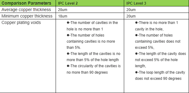
1, the spacing between the wires for mainstream dongguan PCB manufacturer's processing capacity, minimum spacing between wires and wire shall not be less than 4 mil.
Minimum line spacing and line to line and line to bonding pad.
From the perspective of production, the conditional case is the bigger the better, more common is 10 mil.
2, welding plate aperture and welding plate width is the mainstream of dongguan PCB manufacturer's processing capacity, welding plate aperture if mechanical drilling way, minimum shall not be less than 0.
2 mm, if in laser drilling way, minimum shall not be less than 4 mil.
And pore size tolerance according to different plate slightly different, generally can be controlled in 0.
Less than 5 mm, welding plate width minimum shall not be less than 0.
2mm。
If it is a large area laying copper, usually with edge need to be inside shrink distance, usually set to 20 mil.
In PCB design and manufacturing industry, in general, for PCB product mechanical considerations, or to avoid because of the copper bare at the edge of the board may cause such as edge or electrical short circuit happens, the engineer will often large area laying copper block relative to the edge in 20 mil, rather than have been spread to the edge of the plate the copper sheet.
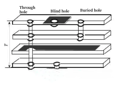
Double sided
PCB circuit board of the copper sheet inside shrink there are many kinds of processing methods, such as edge map keepout layer, and then set up shop copper and keepout distance.
Here introduces a simple method, that is, set different security for laying copper object distance, such as the whole board security spacing is set to 10 mil, and sets the laying copper to 20 mil, can achieve the result of edge inside shrink 20 mil, also likely to die within the copper in addition to the device.
The electric safe distance between text associated film can't do any changes during processing, just D -
CODE is less than 0.
22mm(
8.
66mil)
The following characters everywhere the line width to 0.
22 mm, the character width L = 0.
22mm(
8.
66mil)
。
And the character width W = 1.
0 mm, the height of the whole character H = 1.
2 mm spacing between characters D = 0.
2mm。
When machining printed text is less than the above standard, will be a blur.
A hole to hole spacing of the silk screen is not allowed to cover the welding plate.
For if printing cover the welding plate, on the tin solder printing place will not be able to when wallpapering affecting components.
Circuit board factory in common reserved for 8 mil spacing as well.
If the circuit board area is finite, really do 4 mil spacing and barely acceptable.
If the screen printing cover not carefully in the design of welding plate, circuit board factory in manufacturing automatically eliminate those left on the bonding pad printing part to ensure the welding plate tin.
As a entrepreneur, being trapped in a company under multiple quality problems never appealed to Rocket PCB Solution Ltd..
If you cannot find the specific type of that is best for your business in the above mentioned guide, you can visit Rocket PCB for the best consultants specializing in this field, who can recommend the your are looking for. Customization is warmly welcomed here.
Although the core manufacturing factor of pcb making service is high technology, smart customers know that we need to enhance our material quality and producing standard.