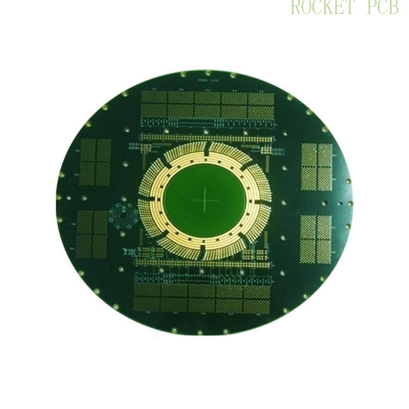
Defects and Solutions of the PCBs
Almost all sorts of high-tech electrical and electronic products are emerging endlessly making increased demand for printed circuit boards. With the increase demand of PCBs quality requirements are also becoming strict. Therefore, meeting the higher standards, PCB manufacturers must comply with the international standards. It is a matter of fact that the PCB technology of PCB manufacturing is very comprehensive and is involving subjects such as fluid mechanics, polymer, photochemical, optics, chemistry, and physics etc. Moreover, it comprises properties of materials such as processing quality, efficiency and stability of equipment and stability etc. The reliability and accuracy of testing is also important which means that issues regarding cleanliness, humidity, and temperature of environment must be catered. Such problems are either directly or indirectly affecting quality of PCBs.
Defects that may arise in PCBs
1.Copper Foil Etching: Sometimes a part of the substrate’ copper foil is etched away due to the restrictions because of changing the substrate for producing dimensional changes when stress is relieved.
Solution: The best solution for the problem is during the process of designing the circuit board, it must be tried to make the board in even distribution. If this is not possible, then some space for transition must be left which would not affect the circuit. This is due to the reason that plank structure of the cloth of glass and density difference of weft is leading to the differences in intensity of longitude to latitude of plank.
2.Brush Plate with Much Pressure: Sometimes, the brush plate is having much pressure due to which the tensile stress is causing pressure leading to base plate deformation.
Solution: The best possible solution for the problem is that brush must be adopted that the parameter of process is in best state as per brush plate. While for the thinner substrate, technology of chemical cleaning must be adopted or even process of electrolysis can be adopted.
3.Resins in Substrate: Sometimes the resins in substrate are not completely cured and are leading to change in dimensions.
Solution: The best solution for the problem is use of baking method. Before the drilling of baking temperature should be set to 1200 Celsius for about 4 hours to have surety that resins have cured for reducing the chances of deformation of the dimensions.

4.Soldering Ball Defects: The soldering ball is one of the most common defects that arise in the surface mount technology-based PCBs. The solder balls are located almost 0.13mm inside of the traces violating the principle of minimum electrical clearance. These are affecting the electrical reliability of the printed circuit boards assembling process. According to the A610 standard of IPC, the ic substrate pcb are considered defective if it has more than 5 solder balls within 600mm2.
5.Root Cause of Soldering Balls: The solder ball can be related to water or air bubble which is trapped withing the soldering paste and when vapor is escaping from paste, it creates ball. The vapor within the soldering paste is escaping so fast that a minor quantity of liquid solder is taken from the joint and then a soldering ball is formed by the times it cools down.
6.Substrate Size: The change in size of substrate weft/warp difference in direction. This occurs because of not paying any attention to the direction of fiber which is resulting in residual stress inside the board’s base, when released its direct impact is on the shrinkage of size of substrate.
Solution: The best possible solution to this problem is determining the change rule of direction of weft/warp as per the compensation of shrinkage of the film. Trim it at same time as per the direction of processing of fiber. Mostly the vertical direction of characters is used for that of the substrate’s longitudinal direction.
Printed Circuit Boards are having water. Water stores inside PCBs in an unexpected humid environment which is not dried before process of assembly begins. Water may store inside as PCB is new and is not enough dried.Water may store inside as beyond needed flux is applied on soldering paste.The preheating temperature might not be high enough for water bubbles to vapor out.Water may store inside because of using an unclean stencil causing the solder paste sticking to unexpected areas.
Solutions: There are certain measures which may be taken for solving this problem. Designing the pads of correct sizes and giving enough spacing as per recommendations identified in datasheets of components.Appropriate increase in the preheating temperature which is also known as reflow profile.Baking the printed circuit board before its printing.The thickness of holes of PCB must be greater than 25μm for avoid the water to trap in to it.
7.Solder Bridging: The solder bridging is more often a phenomenon which is occurring whenever the solder is forming abnormal connection among 2 or more of its adjacent traces, pins, or pads and is forming a conductive path.
Root cause of Solder Bridging: There are numerous reasons of the root cause of solder bridging such as if there is no solder mask among the adjacent pads. In case if the pads are having less spacing among them. If there is residue on the surface of PCB or pads. Using dirty stencil may be causing such problems. Misalignment while process of solder paste printing or placing components on to PCB may also result in solder bridging.
Solution:Adding up solder mask among pads can solve this issue. Design pads and stencil aperture of the right size will overcome the issue. This problem can also be catered by not mixing new and old fluxes together, adjusting the pressure of solder paste printing, adjusting pressure of picking and placing of nozzle, ensuring no gap among stencil and PCB, and cleaning stencil after its use.


