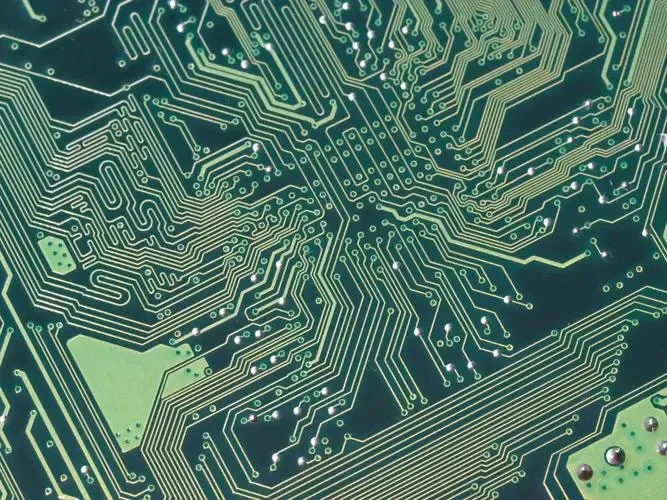
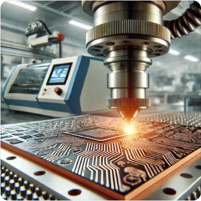
PCB circuit boards of the original title from English (
印刷电路板)
, Chinese translation is called '
printed circuit board,' according to some others PWB (
印刷线路板)
Call it, just as its name implies the product is printing technology to make circuit products.
He replaced the 1940 s, electrical products, in the form of copper wire distribution to make mass production copying speed, product volume shrinking, convenience, unit price lower.
The period of the circuit board is the metal melt cover the surface of the insulation board, make the line.
After 1936, the method of making the insulation of the steering will be covered with metal substrate with corrosion resistant oil ink area selected don't, don't area by etching method, this approach is called (
减去方法)
。
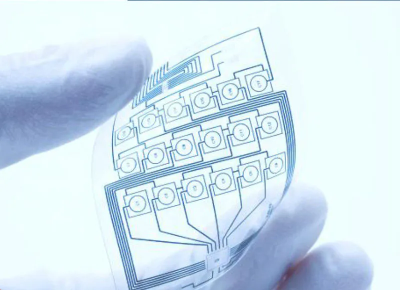
After 1960, record player, tape recorder, video, and other products in the market, gradually adopted double penetration hole of the circuit board manufacturing technology, so the heat resistant and dimension stability of epoxy resin substrate is used in great quantities, still for the production of the main circuit board of the base resin.
PCB circuit boards,
Impedance circuit board)
With the evolution of semiconductor technology, the structure of the electronic products to a higher density.
Electronics assembly is a one-to-one combination structure, when the density of electronic components to improve at the same time, the carrier of element circuit board, of course, also need to improve the link density, it gradually formed a trend of today's high density PCB design.
While raising the idea of layer board since 1967 began have appeared on the product conceptual design, but it wasn't until 1990, IBM published after SLC technology, micro hole technology was gradually mature and practical application.
Before that if no PCB board hole, all designers will adopt the way of multiple pressing higher wiring density, due to the material progress quickly, light sensitivity, the insulation of the photosensitive materials listed in succession, the microporous technology gradually become the main design structure of high density PCB and appeared in many electronic products.
Connection between the circuit layer, in addition to the electroplating, use conductive paste technology link also appear in succession, more prominent, such as: panasonic of ALIVH method and Toshiba B2it published by the method, the technology applied circuit board into high density (
高密度互连,
HDI)
Era.
The main layer board technology development schedules, such as table 1.
1.
To be the best worldwide provider of higher-value pcb making service and the center for quality employment opportunities.
Rocket PCB Solution Ltd. is one of the best provider in China offering online pcb making service consultation and products to boost your
pcb manufacturing services. Visit Rocket PCB and place your order now.
If something seems too good to be true, then it can be a , which provides pcb manufacturing services value over its cost.