Will the popularity of DeepSeek have an impact on the PCB industry?
PRODUCTS
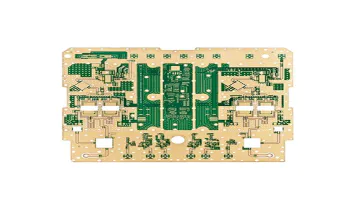
read the brief description of printed circuit board fabrication
by:Rocket PCB
2019-11-22
If you go deep into this theme, you can make custom PCB in several ways.
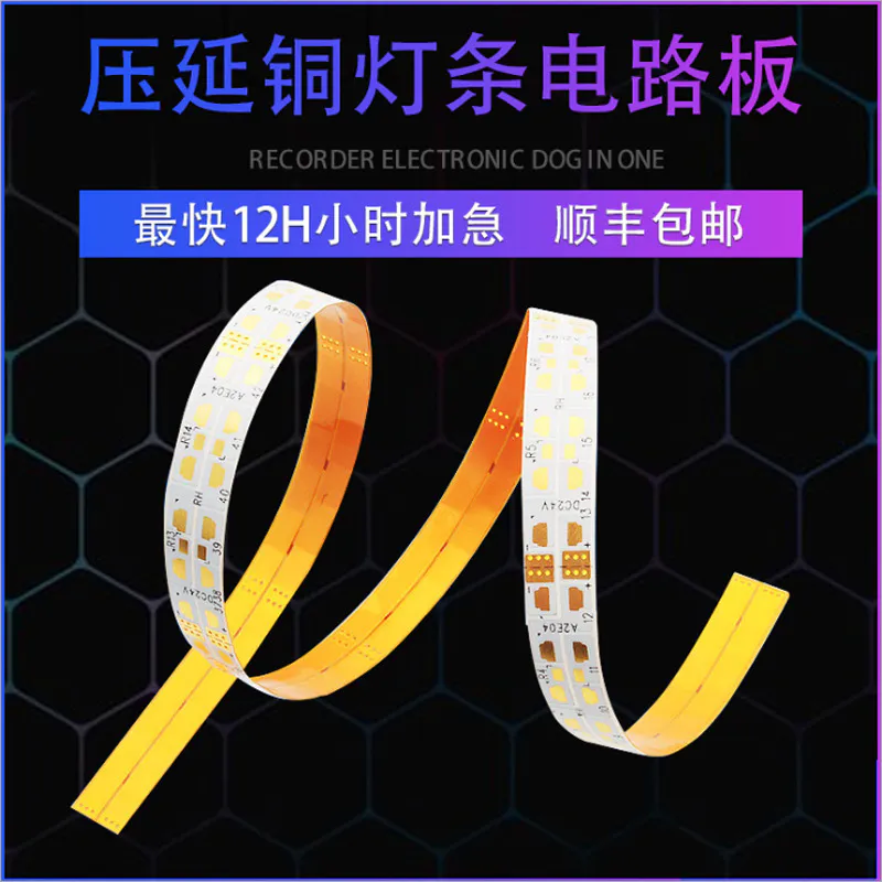
In today\'s market, PCB or printed circuit boards are an essential part of the electronics industry.
This can also be used for satellites, spacecraft and other machines in outer space.
For example, the design of these boards is very flexible.
We also accept orders for any PCB quantity to facilitate ordering and make the process simple and quick.
Because PCB manufacturing technology is very advanced, it becomes more compact every day.
In addition, our knowledgeable staff can provide you with timely customer service.
Adopt a new method :-
To help you place your order quickly and control the production speed, we provide this website.
Although its design is detailed description of the circuit and graphical representation.
In fact, right now, our industry is serving new, efficient printed circuit boards for design layout and different assembly services.
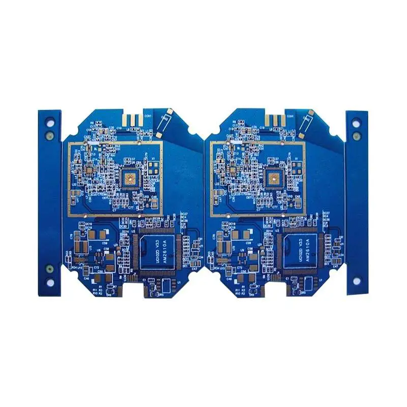
Most of the boards manufactured today are assembled and tested by automated machines.
These services are provided specifically for prototypes, small batch orders, and the turnaround time is fast.
As a result, recently, PCB manufacturing companies have been responsible for adopting new approaches in their designs.
In this case, our organization provides the best quality control.
With this included, you can also get solder mask and legendary printing in various colors for free.
Graphical representation of the circuit :-
If you choose an online board, our engineers will check all your orders before the board is manufactured.
These products were originally made using two types of software.
It is now common to use this CAD software tool to prepare PCB layouts.
With this in mind, the layout produces a graphical representation of the circuit needed to make the PCB.
These programs are computers.
Computer-aided design (CAD)
Software used to design the electronic schematic diagram of the circuit to be generated.
Computer-aided manufacturing, after schematic design (CAM)
PCB prototype was made with software.
Final Connection program :-
To select the material for the Express PCB, different types of objects can be used.
After the selection, the first process is to apply the copper to the entire board.
After that, the circuit layout will be printed on the circuit board through the photosensitive process.
Copper will then be removed from the board using a photo engraving process.
Two processes are used after copper produces traces.
At the beginning, the PCB board without any circuit elements contains a copper trace.
To install the assembly, insert holes through the plating process.
This will create an electrical connection between the layers of the board.
The last step of this process is to screen the board at the appropriate location of the label.
In today\'s market, PCB or printed circuit boards are an essential part of the electronics industry.
This can also be used for satellites, spacecraft and other machines in outer space.
For example, the design of these boards is very flexible.
We also accept orders for any PCB quantity to facilitate ordering and make the process simple and quick.
Because PCB manufacturing technology is very advanced, it becomes more compact every day.
In addition, our knowledgeable staff can provide you with timely customer service.
Adopt a new method :-
To help you place your order quickly and control the production speed, we provide this website.
Although its design is detailed description of the circuit and graphical representation.
In fact, right now, our industry is serving new, efficient printed circuit boards for design layout and different assembly services.
Most of the boards manufactured today are assembled and tested by automated machines.
These services are provided specifically for prototypes, small batch orders, and the turnaround time is fast.
As a result, recently, PCB manufacturing companies have been responsible for adopting new approaches in their designs.
In this case, our organization provides the best quality control.
With this included, you can also get solder mask and legendary printing in various colors for free.
Graphical representation of the circuit :-
If you choose an online board, our engineers will check all your orders before the board is manufactured.
These products were originally made using two types of software.
It is now common to use this CAD software tool to prepare PCB layouts.
With this in mind, the layout produces a graphical representation of the circuit needed to make the PCB.
These programs are computers.
Computer-aided design (CAD)
Software used to design the electronic schematic diagram of the circuit to be generated.
Computer-aided manufacturing, after schematic design (CAM)
PCB prototype was made with software.
Final Connection program :-
To select the material for the Express PCB, different types of objects can be used.
After the selection, the first process is to apply the copper to the entire board.
After that, the circuit layout will be printed on the circuit board through the photosensitive process.
Copper will then be removed from the board using a photo engraving process.
Two processes are used after copper produces traces.
At the beginning, the PCB board without any circuit elements contains a copper trace.
To install the assembly, insert holes through the plating process.
This will create an electrical connection between the layers of the board.
The last step of this process is to screen the board at the appropriate location of the label.
Custom message
Related Products