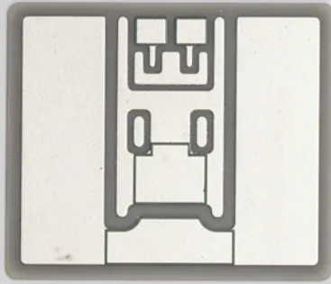
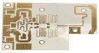
How to Classify PCB Materials
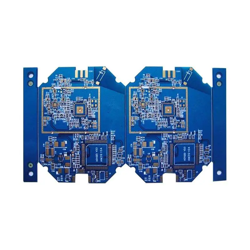
PCB is made of many materials, such as glass fiberboard, paper substrate, metal substrate, plastic substrate, high frequency PTFE, etc.


QUICK LINKS
ABOUT US
CONTACT US
Office: (+86) 755 23040566
Tel: (+86) 158 9965 5195
E-mail: sales@rocket-pcb.com
Skype: Hans@Rocket-PCB
Whatsapp: 86 1589965 5195
Office Address: 2207,Bid 4,He Gu Shan Hui Cheng,35#,Guang Tian RoYanluo street, Song Gang Town,518105 SHENZHENG, CHINA
Plant ADD.: No 69, Lianfeng North Road, Xianxi Area, ChangAn Town, Dongguan, China.


Copyright © 2026 Rocket PCB Solution Ltd. | All Rights Reserved Sitemap Friendship link: CNC machining heat sink