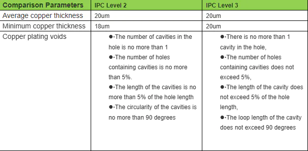
loading

PCB Creation - History and Modern Steps of the

by:Rocket PCB     2020-04-08
Overview A printed circuit board is a fundamental piece of modern day technology. It serves 2 primary functions. First, it holds all of the electrical components of an electronic system. Secondly, it completes the electrical connections between the components. During the PCB creation process, copper sheets are laminated onto a non-conductive board. To transform this 'blank canvas' into something useful, the unwanted copper is etched away to form the connections between various electrical components. History of the Printed Circuit Board Before PCB creation and mass production was developed as a reliable process, engineers used highly inefficient methods such as point-to-point soldering and wire wrapping. Those prior techniques were very time intensive and error prone. In 1936, Paul Eisler created the first printed circuit board as part of a radio. Less than 10 years later, this technology found wide spread adoption in electrical systems. The first generation of printed circuit boards were designed using through-hole (or leaded) components. As the name implies, a hole was drilled in each place on the board that a component lead needed to be inserted. The component lead in each hole was soldered into place. Wave soldering techniques were invented to significantly reduce circuit board assembly time. Modern techniques utilize much smaller components which are called surface mount components. These components have very short leads that do not require holes to be drilled. Modern PCB Manufacturing Steps Step#1 Film Generation: Using computer software, an exact film representation is produced. One film is generated for each layer of the PCB. Step#2 Shear Raw PCB Material: Starting with copper clad board stock, the board is cut to appropriate dimensions. Step#3 Drill Holes for through-hole leaded components: Automated machines drill all holes using carbide drills. Step#4 Electroless Copper Plating: To connect a trace from one side of the board to another, a thin copper deposit is applied in each of the hole barrels. Step#5 Image application: Apply photosensitive plate resist to the bare copper board. Use a light source and film to expose the board. The image is a negative image. This will allow only the unwanted copper material to be etched away. Step#6 Pattern Plate: This is an electrochemical process which places copper on the traces and in the holes. The surface is then tinned with... tin! Step#7 Strip & Etch: Remove dry film from Step #5, then etch the exposed copper. The tin from Step#6 protects the copper signal paths from being etched. Step#8 Solder mask: Apply solder mask area to entire board with the exception of solder pads. Step#9 Apply Solder coat: Apply a solder coat to the pads by immersing the PCB into tank of solder. Using hot air knives the solder is leveled when the circuit board is removed from the tank. Step#10 Labels and Identifiers: Apply white letter markings using a screen printing process. The bare circuit board is now ready for component soldering. This step is often performed in a different facility using 'pick and place' machines. These machines use components that are purchased on a reel to allow for component placement automation. There are many companies that offer PCB Creation and component assembly services. These companies usually offer free board design software that can be downloaded from their site. Give it a try!
Rocket PCB saves time and increases productivity because it's one of the most complete sources of business and contact information.
Make your pcb manufacturing services pcb manufacturing services. Invest in professional pcb service services. For more info, check out Rocket PCB .
On top of making sure all our day-to-day operations are running smoothly, Rocket PCB Solution Ltd. needs to ensure that we're keeping up with all the quality standards of pcb service.
Rocket PCB Solution Ltd. quickly recognized the power of efficient manufacturing and started proactively recruiting people to sell products.
The manufacturing industry is changing fast, so, for Rocket PCB Solution Ltd., being able to pivot and adapt as the marketplace shifts is imperative.
Custom message
Chat Online
Chat Online
Leave Your Message inputting...
Thank you for your attention. Please kindly describe your question first, or please send your inquiry to our email sales@rocket-pcb.com, and we will reply to you ASAP. Welcome, what can I help you?
Sign in with: