Analysis of the current status and future development prospects of the PCB industry market in 2025
PRODUCTS
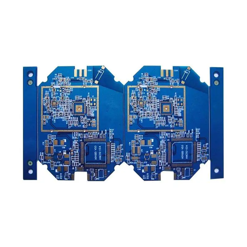
PCB cladding plate technology knowledge
by:Rocket PCB
2020-03-31
Knowledge of PCB cladding plate copper plating technology is a common operation, it is the area on the PCB wiring covered with copper film.
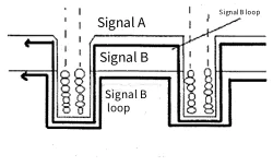
It can improve the anti-interference performance of PCB, called copper coating on the PCB on the unused space as a benchmark, then filled with a solid copper, copper coating can reduce ground impedance, improve the anti-interference ability, reduce the pressure drop, improve the efficiency of power;
In addition, it connected to the ground, reduce the circuit area.
Plating copper needs to solve several problems 1, the different position of a single point of connection, method is to use 0 Ω resistance or inductance connection or magnetic beads.
2, copper plating layer is near the crystal oscillator circuit of high frequency source, method is coated with copper around the crystal, then separate crystal shell vibration.
3, dead zone, if you think you're great, add a hole in the hole will not spend a lot of money.
What are the advantages of copper clad?
Improve the power efficiency, reduce the high frequency interference, one is beautiful!
Large area of copper or copper mesh?
You cannot generalize, why?
Large area of copper clad, if wave soldering, the board may be upward, even bubbles.
From this perspective, the cooling effect is better.
Is usually a high frequency circuit anti-interference requirements of high utility grid, low frequency and high current circuit and other commonly used full copper.
At the start of the grounding line, ground line should go, can't add a hole after dropped COINS package to connect to the pin, the effect is very poor.
Of course, if you choose to use copper mesh, these links some influence on aesthetics.
If you are careful, you can delete them.
Copper and intelligent, this operation will take the initiative to determine copper pouring hole area and the network performance of bonding pad, absolute and you are safe.
It is different from the extraction of copper, extraction of copper without this feature.
Filling the role of copper has a lot of, instead of double panel padding and copper, and connected to the clock, can reduce interference and increase the scope of the ground wire laying low impedance reduction, etc.
So, after the completion of the PCB wiring basically tend to imitation bronze.
Copper wiring note 1, set up the safety of the PCB cladding spacing: the safety of the copper clad spacing is usually a safe distance between two times, but have not been covered in the copper clad, shall be the line setting safe distance between.
Therefore, the safe distance of copper plating layer will also be the wiring a safe distance from subsequent copper plating process, this is different from the expected result.
After a route is good, safe distance expanded to 2 times, and then from a safe distance, after the completion of copper, copper coated back wiring safe distance, the DRC check is not an error.
It can be done, but if you want to rerun the copper, repeat the above steps, the more difficult is that the best way is to set the rules for police safety distance.
The other one is adding rules.
In the clear rules, create a new rule CLEXANG1 can customize (
名称)
And then in the first object matching options box Advestress (
Query)
Standard IUBILDER, click, and then appear 'from BuffueQueDeFabor' dialog, the dialog box the first line of the drop-down menu, select the default showallllevels, conditiontype/operator in the drop-down menu below choose objectkindis, under the right conditionvalue drop-down menu to select a ploy, that will be displayed in the querypreview ispolygon, click the 'ok' to confirm the following is not done, will prompt error completely kept.
Ispolygon inpolygon instead of the next step is to fullquery display box, last modified constraints in need of copper safe spacing, someone said that the wiring rules priority than copper clad priority, copper clad must follow the rules of the wiring safe spacing, need internal wiring rules of copper foil the safety distance between the exception to add, concrete way is in the query NoTimeNo completely.
On the notes.
Actually doing so is unnecessary, because the priority can be changed, the home page of the left corner with an option to set priority rules, the safety of the copper clad spacing rule takes precedence over the above wiring safe spacing rules, each other just way.
2, PCB copper wire width: when copper was chosen in the choice of two modes, set a track width.
If you select the default 8 mil, copper and you connect to the Internet when set the line width range, minimum line width in 8 mil, so when the DRC would be a mistake, the beginning and didn't notice this detail, after each copper clad DRC has a lot of errors.
In the interior of the clear rules, create a new rule CLEXANS1 can customize (
名称)
And then in the first object matching options box Advestress (
Quebug)
, click SudiiabuILDER, then appear BuffugQueDeFabor dialog box, in the dialog box, select the drop-down menu first line showallllevels (
The default value)
Under conditiontype/operator, and then select objectkindis drop-down menu, then choose ploy, on the right side of the conditionvalue polygon shown In right QueRePress view, click OK to confirm the exit, and then did not complete, IsPosion polygons instead of full query display box, In the final step, now you can change your needs In the constraint of spacing.
This will only affect the spacing of copper, not the distance between each layer.
Custom message
Related Products