A, why circuit board is a flat in automation instrumentation online order, printed circuit board if not level off, will cause no, components can't instrumentation to the hole of the board and surface fabrication tray, even crashed automatically installed.
The bent with the components of the PCB board welding, component foot it is hard to cut neatly.
PCB board can't loaded on the chassis or machine outlet, so the circuit board factory met board become warped is also very trouble.
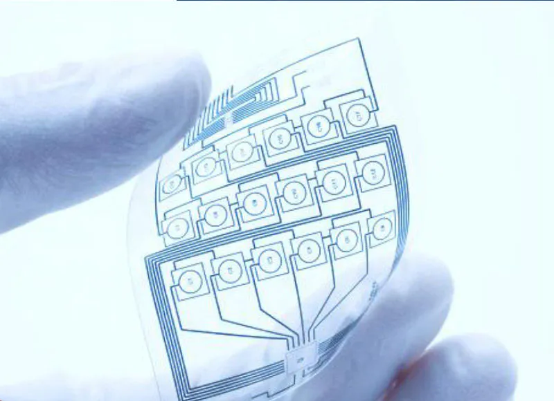
At present, the printed circuit board has entered the era of the surface and chip installation, circuit board factory must be more and more strict with board become warped.
Second, the warp degrees of standard and test method according to the IPC - 6012 (
The 1996 version)
(
Appraisal and performance specification of rigid printed circuit board)
For surface mounting of the printed circuit board allow maximum warping and distortion of 0.
75%, other various boards allow one.
5%.
This is more than the IPC - RB - 276 (
The 1992 version)
Raised on the surface of the printed circuit board installation requirements.
At present, the electronic assembly permission of warp degrees, double-sided circuit board or multilayer circuit board, 1.
6 mm thickness, usually is 0.
70-0.
75%, many SMT and BGA board, request is 0.
5%.
Part of the electronics factory is encouraged to increase the standard of warp degrees to 0.
3%, and the test method of warp degrees follow GB4677.
5 -
84 or the IPC - TM - 650.
2.
4.
22B。
Put the printed circuit board in JingJian fixed platform, the test needle to warp degree of the largest local, to test the diameter of the needle, divided by the length of the curved edge in printed circuit board, warping of the printed circuit board can be calculated.
Three, in the process of manufacturing the plate warping 1.
Engineering design: printed circuit board design should notice: when A.
Multilayer circuit board core board and curing should use the same suppliers of products.
B。
Interlayer half curing arrangement should be symmetrical, 6 layer board, for example, 1 ~ 2 and 5 ~ 6 and a half the thickness of the interlayer and curing piece number should be consistent, otherwise the warps easily after laminated.
C。
On the surface of the outer layers A and B line graphics area should be close as far as possible.
If A is big copper surface, the B side walk only A few lines, the PCB is easy to warp after etching.
If the two sides of the line size difference is too big, can add some independent grid, on one side of the dilute for balance.
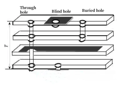
PCB/PCB sandwich plate 2.
Under the baking plate before blanking: copper clad material before baking plate (
150 degrees Celsius, 8 + 2 hours)
Purpose is to remove the moisture inside the board, and make the resin cured within plate, further eliminating residual stress in plate, this is helpful to prevent the plate warping.
At present, many still insist on cutting double-sided circuit boards, PCB baking plate before or after this step.
But there are also some board factory, now the PCB factory baking plate time rules also inconsistent, ranging from 4 to 10 hours, suggested that the class according to the production of printed circuit board and customer demand for warp degrees to decide.
Cut into makeup wait after baking or the whole piece of aniseed materials after drying, the two methods are feasible, suggested baking plate after cutting material.
The inner plate should also be baking plate.
3.
Latitude and longitude of curing to: half piece of laminated curing warp and weft shrinkage rate is different, after blanking and laminated must distinguish between warp and weft.
Otherwise, it is easy to cause finished product after laminated plate warping, even add pressure drying plate is also difficult to correct.
Sandwich plate buckling reasons, a lot of latitude and longitude is half cured when laminated chip to not distinguish, disorderly idea put.
How to distinguish between warp/weft to?
Rolls of half curing the direction of the roll is warp, and width is zonally;
When the long side zonal for copper foil board, short edge is warp, if not sure can contact the
PCB manufacturer or supplier.
4.
: in addition to the stress after laminated multilayer circuit board out after fulfilling the hot-pressing cold-press, cut or milling burrs, then flat on the oven to 150 degrees bake in 4 hours, so that the intraplate stress gradually release and make the resin cured, this step is omitted.
5.
Plate electroplating need straightening: 0.
6 ~ 0.
8 mm thin multilayer PCB panel plating and graphics plating shall be made for special clamping roller, the flying of the automatic electroplating line on the clip on sheet, with a round stick the whole clip roll string on the fly, thus all the boards on straightening roll, so the board will not deformation after plating.
If no such measures, after 20 or 30 micron copper plating layer, thin plate bending, and difficult to remedy.
6.
Hot air cooling after hot air leveling board: printed circuit board is the usual the solder groove (
About 250 degrees Celsius)
Impact of high temperature, should be on the smooth marble or steel plate after natural cooling, after being sent to processor for cleansing.
So good for board prevent buckling.
Some PCB factory to enhance the brightness of the surface of lead, tin, the board into the cold water, immediately after hot air leveling out after a few seconds in the reprocessing, such a fever a cold shock, for certain types of boards is likely to produce warping, layered or blister.
Additional equipment can be mounted on the floating bed for cooling.
7.
Warping board processing: management orderly PCB factory, printed circuit board in the final inspection will be 100% of the flatness inspection.
Who is not qualified board will pick out into the oven, drying under 150 degrees Celsius and weight 3 ~ 6 hours, and natural cooling under pressure.
Then unloading remove the board, in flatness check, so can save some boards, some circuit boards should be two to three times the hot-pressed to leveling.
In use in repair PCB warp Rocket PCB has very good effect.
If above involved prevent warping technology measures were implemented, part of the circuit board hot-pressed also useless, can only be scrapped.
Owing to its
pcb manufacturing services and pcb manufacturing services benefits, has become a buzzword in the pcb manufacturing services market.
Rocket PCB Solution Ltd. plans to produce and execute four marketing seminars, one per quarter, to help business owners see success by sharing important growth strategies and hosting interactive workshops.
Rocket PCB Solution Ltd. employs a numbers of citizens, helping them and their families achieve a higher standard of living.
Rocket PCB Solution Ltd. has developed its range of products around its own market research, which discovers customers' precise needs.