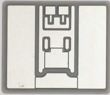
2025 TYPE-C interface new gameplay-desktop display connection interface
PRODUCTS
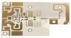
How to easily complete the PCB circuit board design
by:Rocket PCB
2020-07-01
PCB circuit boards, electronic industry is one of the most important parts of almost every electronic device you need to use to it.
Its design can not only directly affect the quality of electronic products, and is closely related to the cost, even can control the success or failure of business competition.
Say simple is not simple, but also said that difficult is easy, just go for it a few steps, can easily complete the PCB circuit board design.
1, pay attention to the PCB circuit board via, welding plate, linear relationship with the gold finger: when wiring hole with solder, on line, gold finger cannot too close, the same property of the hole shall be the gold finger at least 0.
12 mm distance and different properties of hole should be far away from the welding plate with gold finger.
A hole should accomplish minimum external opening 0.
35 mm inner hole 0.
2mm。
PCB circuit boards,
FR4 glass fiber board)
2, pay attention to the size and spacing of the bonding pad: binding pad (
Single line)
Minimal size zero.
2 mmx0。
09 mm90 degrees and the spacing between the solder minimum 2 mils, line of ground wire and the power cord bonding pad width is also required to 0.
2mm。
According to the element at the same time, the binding of bonding pad Angle arrows to adjust the Angle.
3, pay attention to the distance between the welding plate with the original: SMT solder and DIE binding between welding plate and SMT components to keep zero.
More than 3 mm distance, a DIE binding pad with another DIE distance should also keep in 0.
More than 2 mm.
Signal linear minimum 2 mils, spacing of 2 mils, main power supply line do 6 - best
8 mils, in order to enhance the strength of substrate.
4, pay attention to the making craft of substrate: each line must be by electroplating line will use the technique of plating copper casting and forming welding plate and walk the line, even without welding plate network, must be in a certain mode the solder copper plating, otherwise will be the result of the bonding pad without copper.
The above is for sharing by Rocket PCB PCB circuit board design of several important steps.
Memorizing and firmly these steps, to help you journey of PCB circuit board design more walk more far!
Rocket PCB Solution Ltd. has various branches in local businesses, servicing customers and helping to pull in traffic to those businesses.
If you already use pcb making service elsewhere or want the ability to offer restricted chat access to certain individuals, pcb making service pcb manufacturing services offers you the most flexibility.
Further dialogue of Rocket PCB between the approaches, the chapter concludes, could lead to actionable advice on more robust policies that drive both structural change and competitiveness upgrading.
Custom message
Related Products