Five key factors in the design of PCB -
Ding circuit technology
Five key factors in the design of PCB -
Ding circuit technology
by:Rocket PCB2020-04-01
PCB circuit board is the foundation of all electronic design electronic parts, as the main components to support the body, the carrying of all components of the circuit.
The role of the PCB is not only the scattered elements are combined, and ensure that the regularity of PCB design, very good avoid the chaos phenomena caused by artificial ribbon cable and wiring.
About five in the PCB design of power supply design key, is introduced in detail.
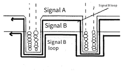
1, the trend of the PCB design needs to have reasonable such as input/output, ac/dc, strong signal, high frequency/low frequency and high voltage/low voltage and so on.
Direction should be inline (
Or separation)
And may not blend.
The main is to prevent mutual interference.
Best is linear, but generally not easy to achieve, is the most unfavorable to ring, fortunately can bring improvement of spacing.
For dc, small signal, low voltage PCB design requirements can be lower.
So 'reasonable' is relative.
2, PCB design, choose good place after place is often the most important, small ground how many what it did for engineering and technical personnel, it serves to show its importance.
Normally require total points, such as: the forward amplifier more than the ground, should meet and then connected to the main land, and so on.
Restricted by all kinds of difficult to fully do it in the reality, but should try to follow.
In practice, however, this problem is quite flexible, everyone has its own set of solutions, if you can target specific PCB explanation would be easy to understand.
3, PCB design, reasonable arrangement of the power filter/decoupling capacitor usually only in the schematic diagram draw some power filter/decoupling capacitor, but they can not point out their respective in where.
Actually these capacitance is for switching devices (
Gate)
Or other need to filter/decoupling components, set up by the arrangement of these capacitors should be close to these components, are far too, there is no work.
When the power supply filter/decoupling capacitors layout reasonable, the pick up location problem is less obvious.
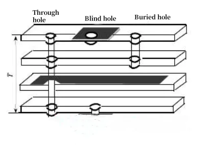
4, PCB design lines buried Kong Tong request the wire diameter hole size should be appropriate to make wide line will never be fine, high pressure and high frequency wire should be smooth, garden must not have sharp Angle, corner also shall not use right Angle.
The ground should be wide, it is best to use a large area of apply copper, the docking site problems has considerable improvement.
Welding plate hole size is too small, or crossed the line or pad size and borehole size mismatch.
The former against artificial borehole, the latter against nc drilling.
Easy to solder drill into 'C' glyph, such as heavy drill out bonding pad.
Wire is too thin, and a large area of no Settings apply copper wiring area, easy to cause corrosion is not uniform.
When not wiring area after the corrosion, corrosion too thin wire is likely, or seems broken off, or completely disconnect.
So the action of the Settings apply the copper is not only increase the ground area and anti-jamming.
Number 5, PCB design via solder joints and linear density of some problems in the early stages of the circuits, it is not easy to be found, they tend to emerge in the later, such as the thread hole is too much, sink copper process will be affected by any carelessness.
So in the PCB design should minimize the thread hole.
Synthetic parallel line density is too large, easily when they are welded together as one.
So linear density should be depending on the level of the welding process to identify, solder joint distance is too small, does not favor the manual welding, only in order to reduce the working efficiency to solve welding quality, or it will leave hidden trouble.
So the solder joints must be taken into account comprehensively determine the minimum distance of the late welding quality and working efficiency.
If you can fully understand and grasp the PCB design considerations, can largely improve the design efficiency and quality of the product.
Will correct the error in the production, will be able to save a lot of time and cost, save the time of rework and material inputs.
A PCB design and design work, can bring certain intangible cost savings for the enterprise.
The above content by: Rocket PCB Solution Ltd, provide a reference for you!
PCB design is good, then you need to find a good PCB board factory to provide you with: PCB proofing, mass production, please keep in mind the following PCB board factory system: Rocket PCB Solution Ltd, quick proofing, professional PCB PCB batch plate, 1 -
34 layer PCB batch production factory.
Can provide a special process or special material top plate plate, welcome to consult customer service for more details.
Thank you for your attention. Please kindly describe your question first, or please send your inquiry to our email sales@rocket-pcb.com, and we will reply to you ASAP. Welcome, what can I help you?
We are here to help you! Please be sure to leave your contact details so that we can better assist you. Or click on the Skype button below to quickly communicate with us.