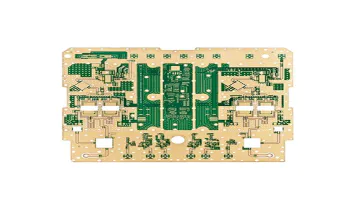
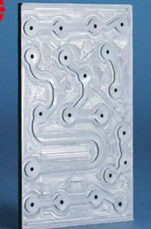
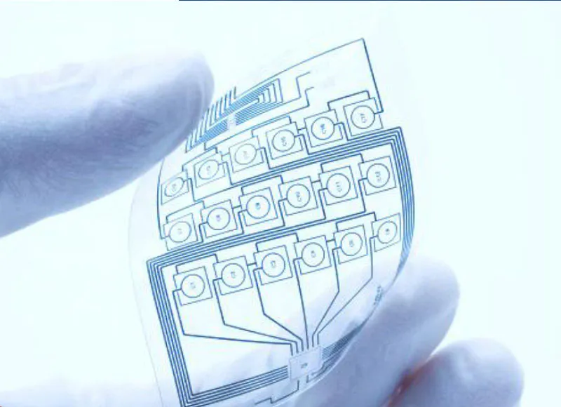
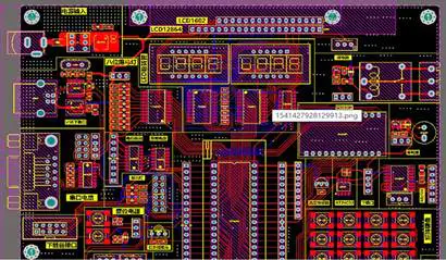
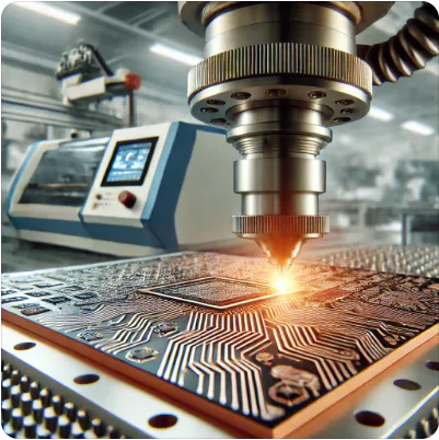
The #1 Reason PCBs Fail Is NOT Your Schematic
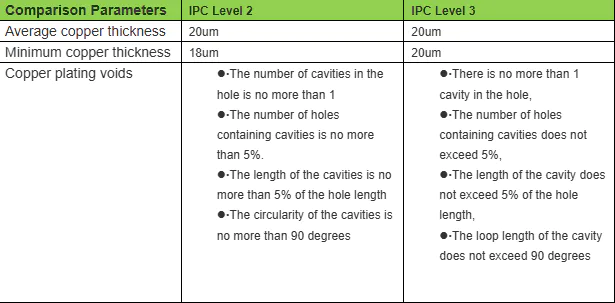
Most engineers blames schematics when a board fails. In reality, over 70% of PCB failures originate from manufacturability decisions made during layout and stack up design - long before facrication starts. Let's break down the real reasons.