This is a general guide to best practice printed circuit boards (PCB)
Design rules for high frequency or RF (RF)circuit.
Following these rules will help you avoid some of the most common pitfalls in RF design.
Poor PCB layout is one of the most common causes of low launch or reception performance and EMC failure due to false launch.
Ideally, engineers engaged in PCB design should be familiar with IPC standards, as they provide a rich source of information and best practices on general principles of PCB design.
When planning to lay out an
rf pcb, first contact the preferred board manufacturer and obtain their guidelines and manufacturing capabilities.
This will include the minimum track and gap width, bit size and other key parameters.
Plate manufacturers should also be able to provide you with their standard layer stack and material data, which will include copper weight, dielectric constant, thickness of the core and pre-
Multi-layer prepreg layerlayer boards.
Unless your circuit is very simple, I would recommend using a 4-layer board, which ensures a continuous ground plane.
When using a dual panel, it is difficult to ensure that the ground plane is notbroken.
Another advantage of the 4-board is the size of the micro-board
The 50 or 75 ohm design belt is easier to manage. Use a micro-
Strip calculator, used to determine the width of the track required for the design impedance, and to make sure that it is within the scope of manufacturing capability, if not, you may need to discuss layers-
Stack with the manufacturer and select a nonstandard build.
Another point to note is that in my experience, trying to maintain separate Netcom for different signal areas often causes problems, not any benefits, this is, to a large extent, a low impedance ground is the safest route.
It is completely acceptable to use FR4 for board upto 2.
Unless the highest level of performance is required, it is 4 GHz.
In some cases, it is worth specifying the board as a controlled impedance in order to provide consistent RF performance.
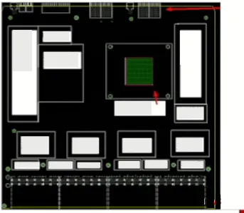
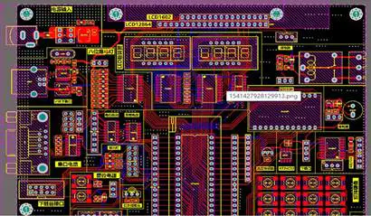
After determining the geometry of the track and board, the next step is to solve the placement problem of the components.
Make sure that the layout of the RF Assembly makes it possible for all RF tracks to remain on the top surface of the minimum length and direction change.
Start from the low signal level area of the antenna or RF input and work backwards to the baseband or digital area.
Keep the digital and power areas away from Analog RF circuits and keep all RF components on one side of the board.
If the RF track cannot run in straight lines, if the CAD system supports oblique bending, use oblique bending, and do not use right angle bending on the RF signal line.
If a series of 45-degree bends or arcs are not supported, this will minimize impedance mismatch, thereby increasing loss and false emission.
On the RF layout, ground flooding is usually provided on the top floor and it is \"stitched\" to the ground by using multiple.
If you intend to do so, make sure that the copper is at an appropriate distance from the RF track and assembly, otherwise the impedance is reduced and the harm is greater than good.
The spacing can be 5-
The distance is 10mm, and there is little benefit by stitching 5mm apart.
The track from the RF assembly to the ground should be as short as possible and 2 or 3 via should be used in parallel to minimize the impedance.