The printed circuit board is an exciting thing.
Every day, you allow us to make our own
printed circuit boards for research projects, everything from personal electronics to airplanes and robots.
It\'s our responsibility to provide him.
Quality products for these important projects.
There are several unique steps in the
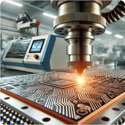
PCB manufacturing process.
This tutorial is used to make circuit boards and you will go through our PCB manufacturing process step by stepsided PCB.
Step 1: The Generation film of all copper and welding mask films is made by photographic methods exposed to Mera.
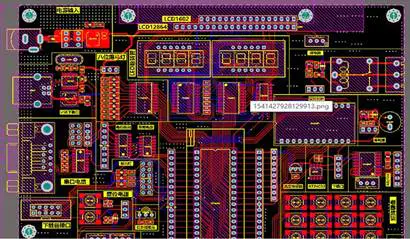
We generate these movies in the design file to create the exact movie (1: 1)
Represent your design
When sending a Gerber file, each Gerber file represents a layer of the PCB.
Step 2: Select raw materials with industry standard 0. 059 \"thick FR-
Copper covered on both sides.
The size of the panel can accommodate many boards.
Step 3: use an automatic drill bit and a hard alloy drill bit to create a drill through the required holes in the printed circuit board based on the files provided.
Step 4: for this purpose, a thin layer of copper is chemically deposited by opening electricity connected to different layers of the OSS.
This copper will later be coated by electrolytic copper (step 6).
Step 5: send photos and images with electronic CAD data to the physical printed circuit board, let\'s start with using photo-sensitive photos to resist panels covering the entire area.
Then the film copper layer of the image (step 1)
Placed outside the ship, high
The UV intensity received detected part of the photoresist.
Then we developed the circuit board by chemical method (
Remove unexposed photos-
Boycott from the panel)
Make mats and tracks.
Step 6: The template form this step is the electrolytic process that establishes the copper thickness on the holes and surfaces of the PCB.
Once the thickness of the copper is established on the circuit and the hole, we form a plate layer and the surface is exposed with an additional layer of tin.
This IPN protects silver and copper during digestion (step 7)
Later removed.
Step 7: The process of saving and etching is carried out in several steps.
First, chemical removal (strips)
Anti-photoresist on the panel.
Then chemical removal of copper (dirty)
Use the panel.
The copper circuit required for the tin protection sensor applied in step 6 is free from contamination.
At present, the basic schematic diagram of OSB has been identified.
Finally, the protective layer for chemical removal of tin (stripped)
The copper circuit of the exposure sensor.
Step 8: welding the mask next, we apply a complete coating on the liquid welding mask layer.
With the help of movies and movies
Intensity of ultraviolet radiation (
Similar to Step 5)
, We carry out the weldable area on the printing board.
The main function of the solder barrier plate is to protect most of the copper circuit of the sensor from oxidation, damage and corrosion, and to maintain the insulation of the Assembly chain.
Step 9: The name of Life (Silk Screen)
Next, we print the Link indicator, logo and other information contained in the electronic file in the panel.
This process is very similar to ink.
But a jet printing process developed specifically for printed circuit boards.
Step 10: then apply the surface to the panel for final surface treatment. This surface (
Tin/lead welding or silver dipping)
Used to prevent oxidation of copper (
Weldable surface)
, Can also be used as a place for welding components on the printed circuit board.
Step 11: Last but not least, we are larger along the perimeter of the PCB from the panel through the NC device.
OSS is now complete and sent to you quickly-
Our lucky customer!