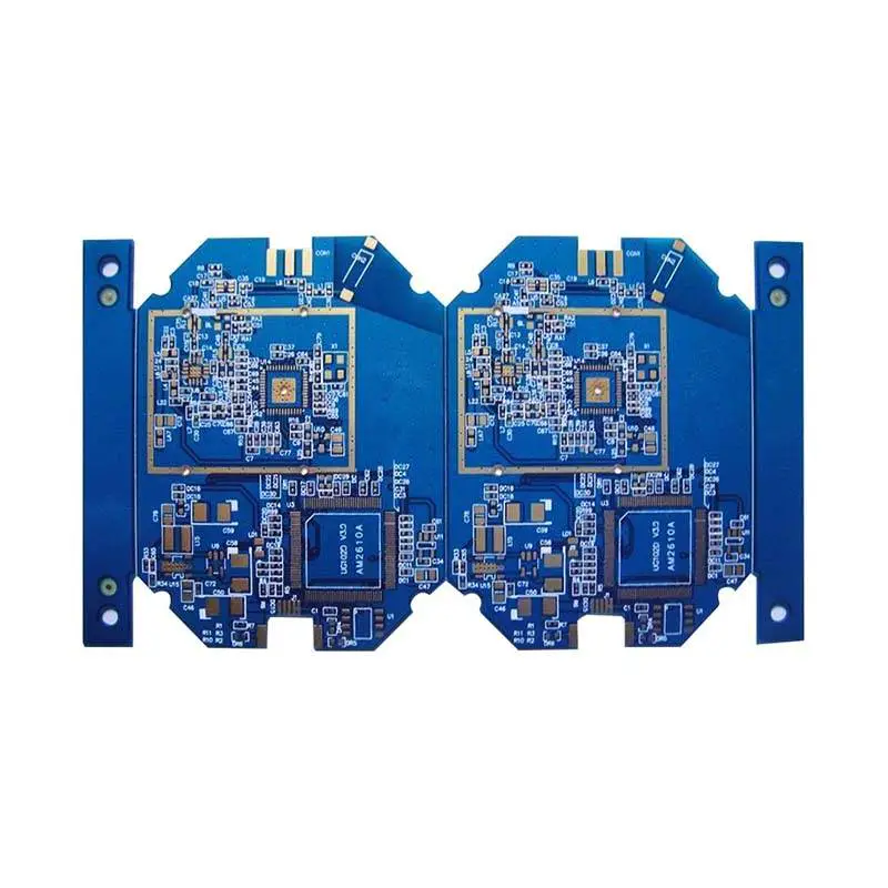
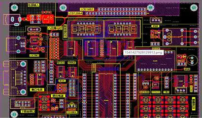
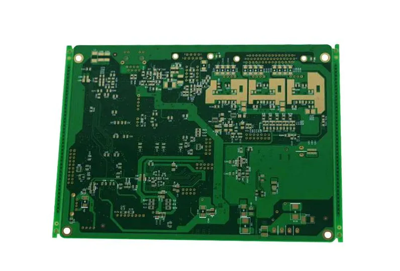
PCB, also known as a printed circuit board, is used to connect electrical components via electricity by using a conductive path and a signal trace.These will have to be etched through laminated copper sheets in order to become non-Conductive substrate.Some PCB filled with electronic components is called a printed circuit board assembly or, simply, a PCB assembly.
For trade reasons, PCBs are present in almost all basic digital equipment.The advancement of
PCB assembly began in the 20 th century.In 1903, a German inventor named Albert Hansen provided a detail about flat foil conductors that were laminated into multi-layer insulating plates.
Also in 1904, Thomas Edison did an experiment on a linen sheet about the chemical strategy of electroplating conductors.In addition, in 1913, a printing-related patent was established in the UK.and-Later, Max Schoop in the United States also got a patent.
In addition, Charles Durcase obtained a patent on the course of forming design for plating circuit design.In order to produce useful PCB components, electrical components must be connected immediately after the PCB is completed.Two construction techniques can be used to ensure the formation of PCB components.
One is throughThe component lead is inserted into the pore structure in the hole, while the other is the surface-Installation structure where the components are located on the pads on the outer surface of the PCB.Both structures have Assembly leads that are mechanically and electrically fixed on the plate through a molten metal weld.In addition, various welding strategies can be designed for the connection of PCB components and the feasibility of PCB assembly.
Mass production should be done by machine placement and bulk wave welding.However, expert technicians are able to weld very small parts by hand with a microscope.This can usually be achieved with tweezers and soldering iron, which consists of an excellent tip and can be used for a small number of prototypes.
However, there are still parts that can\'t normally be welded by hand like a ball grid array.The PCB that constitutes the PCB assembly has a shape-preserving coating, which is applied by dipping or spraying after the assembly has been welded.This coating will fundamentally stop corrosion and current outflow, or short circuit due to the consequences of condensation.
The PCB assembly is responsive to permanent movement, so it must be located in an anti-static bag during transportation.If there is a problem with the processing technology, the component may be damaged because static electricity may be passed by using the circuit board