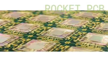
High precision eight circuit board is one of the mainstream products in
printed circuit board now, because of its wiring density is much higher than that of single-sided
PCB circuit boards, and electronic components can be installed on the both sides of the electronic product structure more reasonable, thus once appear quickly replaced the single-sided circuit boards, and become the basic unit of the product to PCB profes sional development, technology is mature, technology is more complicated.
Eight PCB circuit board can provide efficient high-quality single-sided PCB circuit board, double-sided circuit boards, high-precision eight circuit board manufacturers of production.
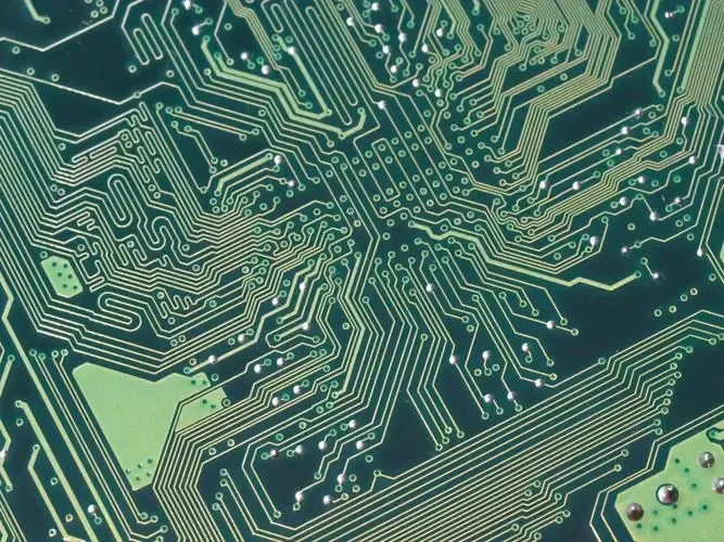
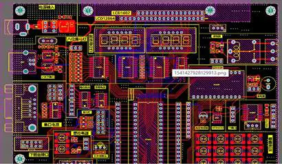
Eight PCB wiring methods: generally, PCB circuit board can be divided into eight layer at the top, bottom and two middle tier.
Top and the bottom line, the middle layer through the command first DESIGN/LAYERSTACKMANAGER ADDPLANE add INTERNALPLANE1 and INTERNALPLANE2 respectively as the use of * such as VCC power supply layer and formation such as GND (
Label that is connected to the corresponding network.
(
Note do not use ADDLAYER, it will add MIDPLAYER, the latter is mainly used for multilayer signal lines placed)
, such PLNNE1 and PLANE2 is two layer connection power VCC and GND copper sheet.
PCB circuit boards,
Impedance circuit board)
Copper sheet without flat will fold, PCB laminated plate using the thin copper sheet frilled opportunities, the higher the more thick copper relative will produce compression effect of nuo flat lower frilled.
If the job has confirmed when copper is flat, that depends on whether the base material of the blank.
If the film produced a large number of flow in the process of melt, can produce copper support sex difference and the possibility of sliding.
So most of the circuit board manufacturers will note that the inner base board line configuration problem, make empty area to avoid excessive.
Most copper crepe fold, will occur on a line density differences of regional, especially designed for large copper surface while there are big empty area location.
In addition, the film (
PP)
Combinations and hot-pressing parameters is also very important.
If improper film composite mobile or producing flow glue, copper slips in melt resin table will inevitably produce crepe fold.
To prevent this kind of problem happen, clamp load of the plate is to focus on homework.
Use load plate design at present, most are highly regulated by sliding block design, the design can be complete in the process of pressure plate to prevent sliding plate, thus cause the frilled would not have happened.
Of film selection, as far as possible within the range may not use the glue content Xie types, and on the pressure and heating rate should also take a low, as long as you can to fill full.
If the production of PCB circuit boards have been buckling, looser conditions in the product specifications, can consider to remove surface copper to make pressing.
Although the plate thickness slightly on the high side, but if the customer specifications can be acceptable, still can be remedied.
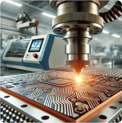
Dongguan Rocket PCB circuit below small make up for the share of high precision eight circuit board processing process: eight copper clad material under a benchmark holes CNC drill guide hole is a test, deburring, scrubbing of electroless plating (
Guide hole metallization)
A full plate thin copper plating, testing scrub screen printing negative circuit graphics, curing (
Dry film or wet film, exposure and development)
An inspection and repairing the plate a line graph electroplating electroplating tin (
Corrosion resistance of nickel/gold)
One to print material,
Photographic film)
A copper etching annealing tin a screen printing a clean scrub resistance welding graphics (
Stick a photosensitive dry film or wet film, exposure, development and heat curing, often heat curing photosensitive green oil)
To clean, dry one screen printing flag character graphics, curing a shape processing, cleaning, in dry electrical on-off testing a tin or organic shielded welding membrane inspection packing the finished products.
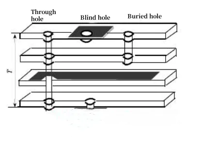
More than eight points through hole and blind holes, a hole from top to bottom through, and the blind hole is only on the top or the bottom one layer, the other is invisible to the layer, that is to say, the blind hole drilling from the surface, but not all layers.
There is a call buried hole, buried hole refers to do the inner hole, is invisible to the table at the bottom.
Do buried holes and the advantage of the blind hole is can increase the line space.
If you have a need for
pcb manufacturing services pcb making service, like , and , you need to be able to find a dependable provider who you can trust when necessary.
To discover more about the
pcb manufacturing services benefits of , go to Rocket PCB .
Rocket PCB Solution Ltd. incorporates average length of the workweek, average growth in number of small businesses, startup per capita, average of growth of business revenues, five-year business survival rate, industry variety, entrepreneurship index and how digital a state is.
The first machine to produce
pcb manufacturing services, the pcb manufacturing services pcb making service was invented in pcb manufacturing services in pcb manufacturing services by pcb manufacturing services and was subsequently improved.
Time is one of the biggest challenges cited by manufacturing pcb making service.