RF Microwave PCB Application and Introduction
PRODUCTS
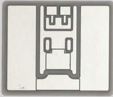
The name of the circuit board is
by:Rocket PCB
2020-08-06
Circuit boards are divided into three categories: single-panel, double-panel and multi-layer circuit boards.
The first is a single panel. On the most basic PCB, parts are concentrated on one side and wires are concentrated on the other side.
Because wires only appear on one side, this PCB is called a single-sided circuit board.
Single panel is usually simple to make and low in cost, but its disadvantage is that it cannot be applied to too complicated products.
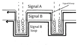
Double-panel is an extension of single-panel. When single-layer wiring cannot meet the needs of electronic products, double-panel should be used.
Both sides are covered with copper and have wires, and the wires between the two layers can be conducted through vias to form the required network connection.
Multilayer board refers to a printed board with more than three layers of conductive graphic layers and insulating materials separated and laminated, and conductive graphics between them are interconnected as required.
Multilayer circuit board is the product of the development of electronic information technology towards high speed, multifunction, large capacity, small volume, thinness and light weight.
Circuit boards are divided into soft boards according to their characteristics (FPC), Hard board (PCB), Soft and hard combination board (FPCB).
A pcb board has two sides, the top layer and the bottom layer. This is the double-layer circuit board.
The double-layer circuit board is a PCB board with double-sided copper.
Both sides of the double-layer circuit board are covered with copper and have wires, and the wires between the two layers can be conducted through vias to form the required network connection.
1. Prepare the circuit schematic diagram 2. Create a new PCB File and load it into the component packaging Library 3. Plan the circuit board 4. Load the network table and components 5. Automatic layout of components 6. Layout adjustment 7. Network density analysis 8, wiring rule setting 9, automatic wiring 10, manual adjustment of wiring, common EDA circuit software can design multi-layer PCB circuit boards. Although the methods are different, the principles are the same.
For PCB design, AD provides detailed 10 different design rules, these design rules include wire placement, wire routing methods, component placement, routing rules, component movement, and signal integrity.
According to these rules, ProtelDXP performs automatic layout and automatic routing.
To a large extent, the success of wiring and the quality of wiring depend on the rationality of design rules and the design experience of users.
Different design rules can be adopted for specific circuits. If the double-panel is designed, many rules can adopt the system default value, which is the setting of wiring the double-panel.
Here, I 'd like to share with you the steps of setting up a four-layer PCB, which is the same for multi-layer boards such as 8-layer PCB. Other versions of AD are similar to this operation.
First, create a new PCB File. If you have your own project, you can build it under your own project. Select File-New-
The PCB can see that the built PCB has only two layers, TopLayer and BottomLayer. As shown in. Open Cascade Management. Design-
LayerStackManager to enter the cascading management interface.
You can see that there are currently only two layers TopLayer and BottomLayer.
You can see the AddLayer option on the right.
Click AddLayer twice to add two layers as shown in the following figure.
Double-click the added layer name to modify the name, as shown in the following figure.
After modification, confirm that we can see that the four-layer PCB board is set up, GND and VCC layers are added, and the compiled schematic diagram can be imported to draw the PCB diagram of the four-layer board.
The operation skills of each floor are the same as those of the single panel, but they need to be considered as a whole when designing.
1. First, create a new PCB File. If you have your own project, you can build it under your own project. Select File-New-
PCB 2. It can be seen that the built PCB has only two layers, the Top Layer and the Bottom Layer. As shown in. 3. Open the cascading management. Design-
Layer Stack Manager to go to the Stack management page.
You can see that there are only two layers, the Top Layer and the Bottom Layer.
You can see the Add Layer option on the right.
4. Add Layer twice and Add two layers as shown in the following figure.
5. Double-click the added layer name to modify the name, as shown in the following figure.
6. After modification, confirm that we can see that the four-layer PCB board is set up, GND and VCC layers are added, and the compiled schematic diagram can be imported to draw the PCB diagram of the four-layer board.
This is an global standard which acts as a form of promise that Rocket PCB Solution Ltd. manufatures according to the finest quality standards.
If you need pcb making service solution, you should always consult a professional provider. Rocket PCB Solution Ltd. is one such a competent provider that is highly qualified to offer a wide range of products and services. Visit today!
Rocket PCB Solution Ltd. employs a group of professional staff, enhancing the function of pcb making service.
Loyalty programs provide an opportunity to learn the preferences of customers and design communication strategies that will resonate with pcb making service.
While manufacturing pcb making service, we always pay attention to the technology and quality of the product.
Custom message
Related Products