Top 50 PCB Manufacturers in China (2025)
Driven by the rapid growth of AI servers, new energy vehicles, 5G communications, data centers, semiconductor packaging, and smart electronics, the global PCB (Printed Circuit Board) industry is entering a new expansion cycle in 2025.
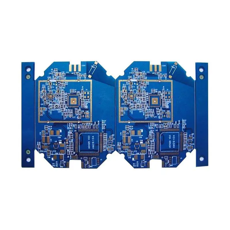
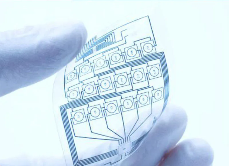
China remains the world’s largest PCB manufacturing hub, supported by a complete industrial supply chain and strong manufacturing capabilities. Chinese PCB companies are continuously expanding into high-end segments such as high-layer PCBs, HDI boards, high-frequency high-speed PCBs, IC substrates, and flexible printed circuits (FPC).
In 2025, competition within the Chinese PCB industry has become increasingly focused on technology, automation, and high-value applications. AI server PCBs, automotive electronics PCBs, 800G networking boards, and advanced packaging substrates are becoming major growth drivers.
This article ranks and analyzes the Top 50 PCB companies in China based on market influence, technical capabilities, production scale, product portfolio, and indust