Get the best performance to make the electronic circuit, electronic circuit board is the circuit component and device in the electronic product support.
Even if the circuit principle diagram design is correct,
printed circuit board design undeserved, also will be harmful to the reliability of electronic products.
Should be paid attention to in the design of printed circuit board, the correct method, comply with the general principles of PCB design, and shall conform to the requirements of the anti-interference design of parts of the layout and setting of the wire is very important.
In order to good quality, low cost of PCB design, should follow the following general principle: first of all, want to consider PCB multilayer circuit board size.
PCB multilayer circuit board size is too large, the printing lines long, impedance increases, the ability to resist noise down, cost also increase;
Is too small, the heat dissipation is not good, and the adjacent lines are susceptible to interference.
In determining the PCB PCB size, then determine the location of the special element.
Finally, according to the function of the circuit unit, for all the components of the circuit layout.
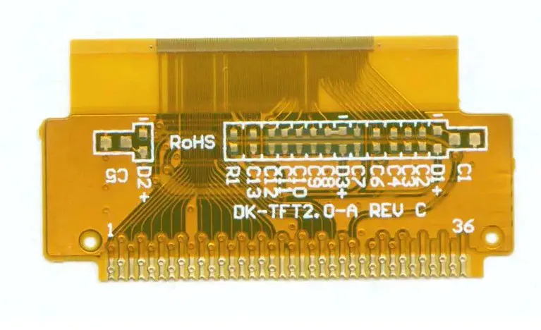
Goldfinger multilayer circuit board PCB circuit boards/when determining the location of the special electronic components to abide by the following principles: 1, should set aside the PCB location hole and fixed bracket position occupied.
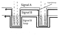
Connection between the two, as far as possible, shorten the high frequency components, try to reduce their parameters and the distribution of the electromagnetic interference between each other.
Vulnerable to the interference of components can't get too close to each other, should as far as possible away from the input and output components.
3, some components or may have a higher potential difference between a conductor, should increase the distance between them, and to avoid discharge lead to accidental short circuit.
With high voltage components should be set in the debugging of the reach of hand.
4, weigh more than 15 g of components, shall be fixed by a bracket for then welding.
Those are big and heavy, calorific value more components, should not be installed on the PCB, and should be installed on the machine chassis backplane, and heat dissipation problems should be considered.
The temperature sensor should be far away from the heating element.
5, the potentiometer, adjustable inductor, capacitor, micro switch adjustable components such as the layout of the machine should be considered the structure requirements.
If the machine adjustment, should be put on the PCB convenient adjustment;
If it is closed to adjust, its position with the position of the adjusting knob on the chassis panel.
For electronic components of the circuit PCB PCB layout, want to accord with the requirement of anti-interference design: 1, according to the process of the circuit arrangement the position of each functional circuit unit, to facilitate signal flow, layout and make the signal as far as possible to maintain consistent direction.
2, work under high frequency circuit, want to consider the distribution of components between parameters.
General circuit should be as far as possible make components parallel arrangement.
In this way, not only beautiful and easy fabrication, easy to mass production.
3, centered on the core of each functional circuit components, layout around it.
Compact components should be uniform, neat, is arranged on the PCB multilayer circuit board.
As far as possible to reduce and shorten the lead and the connection between each components.
4, is located in the edge of the circuit board electronic components, circuit board edge is generally not less than 2 mm.
The best shape for the rectangular circuit board.
Three double as 3:2 or 4:3.
Circuit board face size greater than 200 x 150 mm, the circuit board by mechanical strength should be considered.
However, with the increased prevalence of pcb making service, it has become far more affordable.
More about the most suitable , visit Rocket PCB to get your offer!
If we avoid overselling pcb making service
pcb manufacturing services and capabilities, you gain credibility and earn trust. We did not want to jeopardize our ingrained preference for humility.
Did I make the right decision? Am I saving money? Would I do it this way again? Yes, yes and yes if you choose to visit Rocket PCB and make your enquiry.
We want to be careful and deliberate about developing Rocket PCB, from the platform we choose, to the way we approach it, to the methods we use.