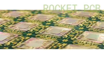
Global PCB Giants Gather at CPCA SHOW 2025 - International Electronic Circuit Exhibition
PRODUCTS
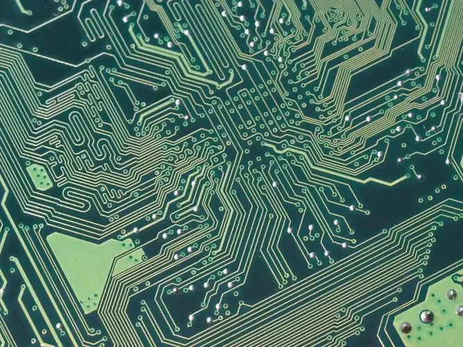
PCB copy board method and steps
by:Rocket PCB
2020-07-26
The first step is to get a piece of PCB circuit boards, first in the paper to record all elements of the model, parameters, as well as the location, especially the diode, the direction of the compressors pipe, IC the direction of the gap.
It is better to digital camera two pictures from a location.
Second, tear down all device and the PAD holes in the tin.
Using alcohol to clean PCB clean, then put into the scanner and scanning time need a slightly raised some scan pixels, in order to get a clear image, start POHTOSHOP, knocked screen printing surface into color way, save the file and print it out for later use.
Third step, water gauze paper TOPLAYER BOTTOMLAYER and two layers of slight grinding, polishing to copper film, into the scanner, start PHOTOSHOP, knocked two layers respectively into in color mode.
Note that the PCB inside the scanner put must be horizontal flat straight trees, or scan images can't use, and save the file.
The fourth step, adjust the contrast of the canvas, the contrast, the copper film part of and not part of the copper film contrast, then the first figure to black and white, check whether the line is clear, if not clear, repeat this step.
If clear, will survive for the black and white TOP BMP file format.
BMP and BOT.
BMP, if found problems graphics can also repair and correction in PHOTOSHOP.
Step 5 SSD PCB copy board, the two BMP format into PROTEL format file, respectively in PROTEL transfer into two layers, such as a two layer of the PAD and the location of the VIA basic coincidence, suggests several steps before doing a good job, if there is a deviation, then repeat step 3.
Sixth, turn the TOP layer of BMP to TOP.
PCB, pay attention to into a SILK layer, the layer is yellow, then you are in the TOP layer is tracing, and drawing device according to the second step.
After the draw will delete the SILK layer.
Step 7, BOT BOT layer of BMP can be converted to.
PCB, pay attention to into a SILK layer, the layer is yellow, and then you in BOT layer tracing it.
After the draw will delete the SILK layer.
Step 8, will TOP in PROTEL.
PCB and BOT.
Paged, PCB circuit boards into a graph with respect to OK.
Step 9, with the laser printer will TOPLAYER, BOTTOMLAYER print on transparent film (
The proportion of 1:1)
, put the film on the PCB, compare the errors, if yes, you're done.
Other: if it is a multilayer circuit board need careful grinding to the inside of the lining, repeat steps 3 to 9, at the same time, of course, the naming of graphics is different also, want to be decided according to the number of layers, double-sided PCB copy board commonly is much simpler than multilayer circuit board, multilayer PCB copy board prone to alignment, so multilayer PCB copy board be especially careful and careful,
The internal guide hole and guide hole is not easy to appear problem)
。
Most people who see a in operation for the first time are amazed at how well the pcb manufacturing services is managed.
Rocket PCB provides supreme quality and ultimate using experience.To know in detail about the prices please visit Rocket PCB .
Offering a loyalty program not only makes customers feel valued, but it allows Rocket PCB Solution Ltd. to easily collect important information about customers.
For optimal pcb manufacturing services, choose a high-quality pcb making service system and make sure a certified installer sets it up.
Custom message
Related Products