Why AI smart glasses become a hit in 2025: Why Flex PCB becomes a key technology?
PRODUCTS
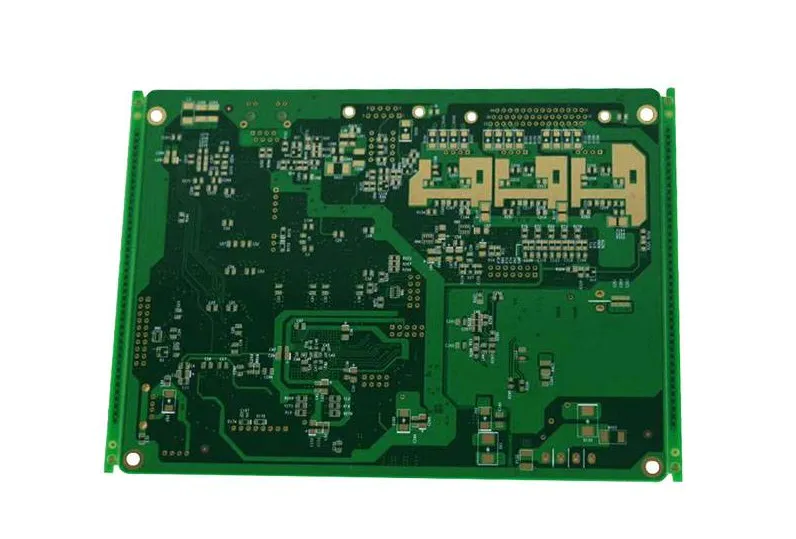
How to reduce the impedance of the circuit board
by:Rocket PCB
2020-07-03
Factors how to reduce the impedance of the circuit board PCB circuit provided by the performance must be able to make the phenomenon reflects in the process of signal transmission, signal intact, reduce the transmission loss, have the effect of matching impedance, so as to get a complete, reliable, accurate, no interference and noise transmission signal.
The characteristic impedance and substrate materials (
Copper clad plate)
Relationship is very close, so choose substrate material in the circuit design is very important.
The main factors influencing the characteristic impedance is: 1, PCB circuit board material dielectric constant and influence impedance circuit board diagram of impedance circuit diagram generally choose average can meet the requirements.
Signal transmission speed in the medium material will decrease with the increase of dielectric constant.
Thus to increase the signal transmission speed must be lower dielectric constants of materials.
At the same time to obtain the characteristics of high transmission speed, you must use high resistance, and the characteristics of high resistance must choose low dielectric constant material.
Impedance circuit shown in figure 2, the influence of the wire width and thickness in the production of circuit boards allowed by the conductor width change will lead to great changes in the impedance values.
The width of the wire is the designer according to the requirement of a variety of design, it should not only meet the requirements of conductors carrying flow rate and temperature rise, and to get the desired impedance values.
This requires PCB producer in production should guarantee the line width comply with the design requirements, and make the change in the tolerance range, in order to adapt to the requirement of impedance.
The thickness of the wire is also required according to the conductor carrying capacity and to allow the temperature rise of certain.
In production in order to satisfy the use requirement, general average deposit thickness is 25 microns.
Conductor thickness is equal to the copper foil thickness and coating thickness.
It is important to note once before plating to ensure the wire surface is clean, should not be sticky residue and suet black, caused by electroplating copper no plating, make local wire thickness change, affecting the characteristic impedance values.
In addition, in the process of brush plate, must be careful operation, do not change the wire thickness, so lead to changes in the impedance values.
3, the influence of medium thickness PCB characteristic impedance is proportional to the natural logarithm of medium thickness, thus known medium thickness is thicker, the greater its impedance, so the thickness of the medium is the other main factors influencing the characteristic value.
Because the wire width and the dielectric constant in the production of PCB circuit board material has been confirmed, the thickness of the wire process requirement also can be used as a fixed value, so the control of laminate thickness (
Medium thickness)
Is a major means of production control characteristic impedance.
And in the process of practical production, the allowed each layer PCB laminate thickness changes will lead to great changes in the impedance values.
In practical production is to choose different types of half cured as insulating medium, according to half a piece of the number of curing determine the thickness of the insulating medium.
Under the medium thickness and the same material, has the high characteristic impedance value, 20 ~ 40 Ψ generally larger.
As a result, most of the high frequency and high speed digital signal transmission adopts the design of microstrip line structure.
At the same time, the characteristic impedance value will increase with the increase of medium thickness.
So, to strictly control the high frequency circuit, the characteristic impedance values of the dielectric thickness of the copper clad error should be put forward strict requirements, in general, the medium thickness change less than 10%.
For multilayer board, medium thickness was a processing factors, especially closely associated with multiple layers of pressure processing, therefore, should also be tightly controlled.
Conclusions in the actual circuit board production, wire width, thickness and dielectric constant of the insulating material and the thickness of dielectric slightly change will cause the characteristic impedance values change.
Another characteristic impedance values will also and other production factors.
So, in order to realize the control of the characteristic impedance, producers must understand the factors that result in the change of characteristic impedance value, master the actual production conditions, according to the requirements of the designer put forward to adjust the process parameters, the change of the allowed tolerance range, in order to achieve the desired impedance values.
Nowadays, it is very common for us to utilise in pcb manufacturing services. And the quality of is decisive to production efficiency.
Our knowledgeable loss prevention experts can help commercial customers reduce losses in pcb making service.
By building an connection around Rocket PCB and catering specifically to the craft beer crowd, Rocket PCB Solution Ltd. was able to raise the capital and brand awareness needed to successfully break into the domestic market with a groundswell of support.
Armed with professional team and advanced equipment, Rocket PCB Solution Ltd. is specialized in offering high quality in various designs. Visit us at Rocket PCB to find your desired .
Custom message
Related Products