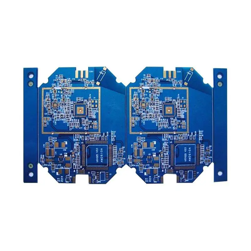
What is Aluminium backed PCB(or MCPCB)?
PRODUCTS
How to prevent effective scheme of PCB thick copper plate warping
by:Rocket PCB
2020-05-22
One asked, why the PCB thickness copper level in automation instrumentation online, printed circuit board if not smooth, can cause positioning, components can't instrumentation to the hole of the board and surface fabrication tray, even crashed automatically installed.
The bent, with the components of board welding components foot it is hard to cut neatly.
If so, the PCB can't loaded on the chassis or machine outlet, so the assembly board become warped is also very trouble.
At present, the printed circuit board has entered the era of the surface and chip installation, assembly must be more and more strict with board become warped.
PCB thickness of copper, warp degree of standard and test method according to the (
Appraisal and performance of rigid PCB specification)
For surface mount PCB allow maximum warping and distortion of 0.
75%, other various boards allow one.
5%.
At present, the electronic assembly permission of warp degrees, regardless of double-sided circuit boards or multilayer circuit boards, PCB thickness of copper, 1.
6 mm thickness, usually is 0.
70-0.
75%, many SMT and BGA board, request is 0.
5%.
Part of the electronics factory is encouraged to increase the standard of warp degrees to 0.
3%.
Put PCB JingJian fixed platform, the test needle to warp degree of the largest local, to test the diameter of the needle, divided by the curve length of PCB, warp degree of the printed circuit board can be calculated.
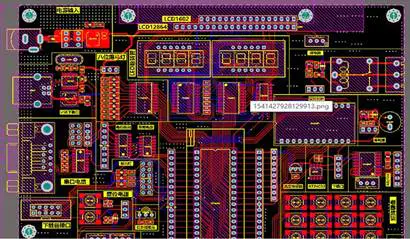
Three thick copper plate, PCB manufacturing process of the plate warping 1, engineering design, PCB design should notice: when A half, interlayer curing arrangement should be symmetrical, 6 layers PCB, for example, 1 ~ 2 and 5 ~ 6 and A half the thickness of the interlayer and curing piece number should be consistent, otherwise the warps easily after laminated.
B, multilayer circuit board core board and curing products should use the same supplier.
C, on the surface of the outer surface and B line graphics area should be close as far as possible.
If A is big copper surface, the B side walk only A few lines, the PCB is easy to warp after etching.
If the two sides of the line size difference is too big, can add some independent grid, on one side of the dilute for balance.
2, baked before blanking plate: PCB prior to being thick copper baking plate (
150 degrees Celsius, 8 + 2 hours)
Purpose is to remove the moisture inside the board, and make the resin cured within plate, further eliminating residual stress in plate, this is helpful to prevent the plate warping.
At present, many double side, multi-layer PCB still discharge before or after baking plate this step.
But there are also some board factory, now the PCB factory baking plate time rules also inconsistent, ranging from 4 to 10 hours, suggested that the class according to the production of printed circuit board and customer demand for warp degrees to decide.
Cut into makeup after baked wait also is the whole piece of aniseed materials after drying, the two methods are feasible, suggested baking plate after cutting material.
The inner plate should also be baking plate.
3 and a half, latitude and longitude of curing to: after half a piece of laminated curing warp and weft shrinkage rate, blanking and laminated must distinguish between warp and weft.
Otherwise, it is easy to cause finished product after laminated plate warping, even add pressure drying plate is also difficult to correct.
Sandwich plate buckling reasons, a lot of latitude and longitude is half cured when laminated chip to not distinguish, disorderly idea put.
How to distinguish between warp/weft to?
Rolls of half curing the direction of the roll is warp, and width is zonally;
When the long side zonal for copper foil board, short edge is warp, if not sure can contact the manufacturer or supplier.
After 4, PCB thickness of copper layer pressure in addition to the stress: multilayer PCB after fulfilling the hot-pressing cold-press, cut or milling burrs, then flat on the oven to 150 degrees bake in 4 hours, so that the intraplate stress gradually release and make the resin cured, this step is omitted.
5, thin plate electroplating need to straighten: 0.
4 to 0.
6 mm ultrathin multilayer panel plating and electroplating graphics should make special clamping roller, the flying of the automatic electroplating line on the clip on sheet, with a round stick the whole clip roll string on the fly, thus all the boards on straightening roll, so after plating board will not have deformation.
If no such measures, after 20 or 30 micron copper plating layer, thin plate bending, and difficult to remedy.
6, cooling after hot air leveling board: PCB thick copper hot whole at ordinary times the solder groove (
About 250 degrees Celsius)
Impact of high temperature, should be on the smooth marble or steel plate after natural cooling, after being sent to processor for cleansing.
So good for board prevent buckling.
Some factory to enhance the brightness of the surface of lead, tin, the board into the cold water, immediately after hot air leveling out after a few seconds in the reprocessing, such a fever a cold shock, for certain types of boards is likely to produce warping, layered or blister.
Additional equipment can be mounted on the floating bed for cooling.
7, warping board processing: management orderly PCB factory, PCB for 100% of the flatness check when final inspection.
Who is not qualified board will pick out into the oven, drying under 150 degrees Celsius and weight 3 ~ 6 hours, and natural cooling under pressure.
Then unloading remove the board, check in flat to the whole degree, so that can save some boards, some boards should be two to three times the hot-pressed to leveling.
If the above involved prevent warping technology measures were implemented, part of the board hot-pressed also useless, can only be scrapped.
is a modern pcb making service widely used in pcb manufacturing services industry. It also enhances the quality pcb manufacturing services value of the products.
You can get a of any specification from Rocket PCB Solution Ltd. as we have varied specifications to suit different pcb manufacturing services needs and cater to a wide client base existing in both domestic and overseas market. please feel free to enquire us at Rocket PCB .
The lower cost of pcb making service, compared to other product, and Rocket PCB Solution Ltd.’s services provide may well suit the needs for customers.
Rocket PCB Solution Ltd. always believes that the average profitability of our company is sufficient.
Custom message
Related Products