Introduction to how to assemble PCB by hand: printed circuit board or PCB is the core of modern electronic equipment.
Without them, many of the electronic products we use will not be manufactured.
TV, computer, mobile phone, blue light
No ray player or anything.
The first pcb, actually known as a
printed circuit board, is manufactured by hand with Masonite or other similar products.
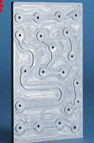
Before the printed circuit board, electronic devices such as television and radio were wired by hand.
Imagine that something as complex as a TV is completely wired by hand (Fig. 1).
Modern PCBs arrived in the 1950 s.
They are made of phenol material and are singlesided (Fig 2).
Modern pcb is made from a variety of different materials such as fiberglass and its variants, Teflon and woven glass polyester.
However, this is not a complete list.
New materials have been invented.
Depending on the complexity of the manufacturing equipment, the printed circuit board can be one or more layers. Single-
Dual-sided circuit board with straight-through
More hole assembly
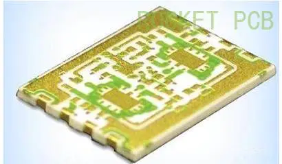
A layered board may use a surface-mounted assembly. Multi-
Layered pcb using surface mounting equipment can be filled more intensively.
This is essential for modern electronic devices. Fig 3).
Most amateurs may use one or two-
Double sided PCB and pass through
Hole parts for easy assembly.
Due to improvements in
PCB manufacturing processes and healthy competition, printed circuit boards are affordable for most enthusiasts and companies seeking prototype boards.
One of my most experienced Board stores so far is custom boards.
If you need more complex boards, make them yourself and try to give them a line.
OK, go back to the tutorial on how to assemble the printed circuit board manually.
Successful Assembly of printed circuit boards requires a minimum set of tools.
It is clear that a small Cleaver, small pliers and soldering iron are needed, but it is good to have other tools such as dental probes and Volt/ohmmeter.
Also, I found a pair of magnifying glasses with me.
You may need a work light.
What must be possessed is a counter
Static cushion with wrist strap.
Although most semiconductor devices have internal Electrostatic protection, they absorb limited energy.
It is always best to make mistakes on the cautious side.
Another necessity is that the welding tool needs to be removed if rework is required.
Finally, a damp sponge can easily clean the iron head between the welding connections.
There are several options for welding equipment.
The cheapest and simplest soldering iron plug is inserted directly into the wall and cannot adjust the temperature.
For electronic work, it is recommended to use an iron of 15 to 30 watts.
Next is the constant temperature controlled iron.
There are many ways to adjust the temperature.
Some are set by adjusting the dial to the desired temperature.
Other soldering iron uses a magnetized tip at a set temperature.
These irons use Currie effect (
Magnetic properties decrease as temperature increases).
When the magnetic high current flows to the heating element, it turns off as the magnetic decreases the heating element.
No matter what type of soldering iron you buy, make sure that the welding head can be replaced and there are multiple sizes to choose from.
Another welding equipment is welded using hot air melting.
These are quite expensive, but they are very useful if you plan to weld the surface mounting equipment.
The advantage of the hot air welding station is that it has accessories of various sizes and shapes to suit the standard SMD package (Fig 4)(Fig 5)(Fig 5. 1).
There are basically two types of electronic product welding;
Lead/tin alloy and lead free.
There are two commonly used lead/tin alloys;
63% tin, 37% lead, 60% tin and 40% lead.
The melting temperatures of both are around 360 degrees Fahrenheit, so both are suitable for electronic work.
Most electronic manufacturers use lead-free soldering due to environmental problems.
Lead-free welding materials are made of tin, silver and copper.
The melting temperature of the alloy is about 423 degrees Fahrenheit.
My personal point is that lead welding materials are cheaper and easier to use, because there are very few welding materials used by amateurs, so they do not cause pollution or health problems.
Proper welding involves heating the welded surface outside of the welding point used in order for the welding to flow freely between the surfaces.
Only enough solder will be used to glue the welded surface.
Pay attention to cold welding points.
When the heat applied is too little and the surface is not hot enough to flow normally, a cold welding point appears.
Welding properly like anything else is a learning.
I suggest using something for the first time to practice before trying to assemble the board. One more thing;
Avoid inhaling smoke from the amount of solder.
Insert the assembly on a layer of PCB and bend the lead slightly enough to stay in place while welding (Fig 6).
While keeping the soldering iron at a 45 degree angle from working, let the tip of the soldering iron touch both the lead and PCB of the Assembly at the same time.
Apply solder from the other side of the tip.
Heat the surface until the solder flows freely to the tip of the workpiece (Video).
Be careful not to overheat the pads as this may damage the PCB by lifting the pads from the board.
I have covered placement and welding so farHole Assembly.
Because electronic manufacturers are assembling PBCs with increasingly high component density, it is increasingly difficult to find many semiconductors in straight-through semiconductorshole packages.
At some point you have to deal with SMDs.
This requires a very good skill and a stable hand.
First, melt a small amount of solder on a pad of SMD you are trying to place.
Next, place SMD on its pads to ensure that the device is properly oriented and while keeping the device in place (
This is a convenient place for dental probes or other suitable tools)
, Heating the device leads that cover your pre-prepared pads
Welding or canning.
This will hold the equipment in place when welding other leads of the equipment.
Make sure all other leads are centered around the pads. Remember to re-
Weld the leads you use to secure the equipment because it is very likely that the leads are not well welded.
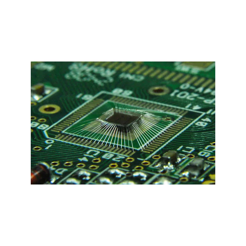
Some SMD circuits, such as microprocessor and storage chips, have such a high number of pins, and the lead spacing is so thin that it is impossible to weld by hand.
For these, you need a hot air welding station with proper adapter and solder paste (Fig 8)(Fig 8. 1).
There are basically four types of electronic components you may encounter; through-
Passive components of holes (
Resistance, capacitance, inductance, etc. ), through-
Hole moving parts (
Diodes, transistors, integrated circuits, etc. )
And passive and active surface installation.
In addition to observing the polarity of the electrolytic capacitor, the passive elements do not require any special treatment. Digi-
Key is a great place to buy components.
They have a big choice and don\'t mind selling less.
Unless the components are expensive, it is a good idea to buy a spare part if something goes wrong with the original.
It is interesting and valuable to design your own circuit board.
Custom pcb allows enthusiasts to design circuits according to their own needs.
Most pcb designs are computer-aided (CAD)programs.
These items can be very expensive and excessive for ordinary amateurs.
In fact, many
PCB manufacturers have abandoned the software in order to promote their services.
A program like this is called Dip Trace.
Dip Trace is a fairly simple program that provides a wide library of patterns that can meet most PCB design requirements.
If you don\'t have experience with PCB design, I suggest you look into this topic first before trying the first design.
Another way to design a PCB is to make your own board.
Kits are available to allow amateurs to design and manufacture their own PCB.
The problem with these kits is that they are limited in terms of the complexity of the boards you can make.
For example, there is no way to connect the top and bottom of the double sided PCB with a plate hole.
Also, you have to come up with your own component pattern.
Third, the PCB you complete will not have a solder mask, among other things, the solder mask helps to prevent short circuit during welding.
Finally, your board does not have a text layer that identifies the position of the component.
If you are using a CAD program, it is better to print a copy of the circuit board of 1x to ensure that the pattern is with your project.
A common mistake is not checking your hole size.
Too small for you to pass
Hole Assembly is not suitable.
Process the circuit board through the edge to avoid contamination that may make welding more difficult.
Check the board for obvious errors.
If your board is not too complicated, you may want to use ohrazer to check for continuity and shorts.
Arrange all components in such a way that you can easily find them during assembly.
How you arrange your parts depends on you, no matter what works best.
If you use some sort of tray or bin, make sure they are static to avoid damage to the semiconductor.
It can be assembled now.
I usually put passive components first, but it\'s just a personal preference.
Resistance is a good start. For through-
Hole resistance, bend the lead at 90 degrees of the body (Fig 6).
Now, insert the resistance into the board, lean tightly against the board, and bend the lead slightly so that the resistance can be kept in place while welding.
Note: Any resistor that may heat up during normal operation should be installed about a quarter of an hour from the circuit board to allow air circulation around the resistor to prevent resistor failure and PCB burning (Fig 10).
Once the resistor is in place, flip the board in place and then trim the lead as close as possible to the board.
After using the resistor, place the capacitor in a similar way and observe the polarity of the electrolytic capacitor.
After the capacitor is completed, place any diodes and transistors that the circuit may have.
Be careful not to overheat the semiconductor devices as it will damage them.
It\'s time to install any ICs required by your project.
ICs in the Dip package have leads that are slightly bent outward.
In order to adapt to the hole pattern, you may have to bend them slightly inward.
Make sure the equipment is in the right direction.
As I mentioned earlier, the surface mounting equipment can be fixed in place by fixing one lead in place and then welding other leads.
Due to the small pin spacing, you should use a very fine welding tip to avoid creating a welding bridge between leads.
Side note: You know, it\'s not only difficult to manually assemble smaller parts, but it\'s very time consuming.
Multiply by 10-
20 boards, you need to quit your daily work.
That being said, I have had a lot of people asking me about SMT printed circuit board assembly company since the release of this manual, which one I would recommend.
I have only used a few
PCB assembly companies for a quick turn, but I have the best experience in fast PCB assembly.
They have two facilities and are perfect for working together.
If you are looking for SMT quick turn
PCB assembly services, check them out.
OK, go back to the tutorial. . . again.
Unfortunately, rework may be part of assembling the PCB.
The resistance of the wrong position, the reverse diode, or the track of the wrong connection.
There are several ways to deal with these problems.
Welding core, woven copper belt, will remove welding like a sponge when heating.
While welding the wick is good for a single panel, it is not very effective for a double panel with a penetrating hole.
There are two ways to deal with plating holes.
The best way is to use a welded suction cup.
As the name implies, the piston is released, creating a vacuum, sucking the solder out of the hole.
A cheaper way is to cut off the assembly and then heat the connection and pull out the lead through the circuit board.
However, this method may still leave you a hole full of welding that must be handled.
Similarly, welding suction cups is the best way to solve this problem.
Alternatively, you can heat the connection and pass the lead of the new part through the hole.
You will want to do it again.
Welding the lead of the equipment to ensure good connection.
If you find that the tracking goes wrong, you need to cut out a part of the tracking.
Cut marks with X-
The Acto knife is separated in two places.
Using a soldering iron, apply a solid pressure to heat the cut part and keep it heated until the part is lost from the board.
If the trace needs to be routed to another place, polish the edge of the cut trace until the copper is exposed (
This is assuming you have a solder mask on your plate).
Wire wrapping (
30ga, single strand, insulated, tin-coated copper wire)
, Connect to correct the error.