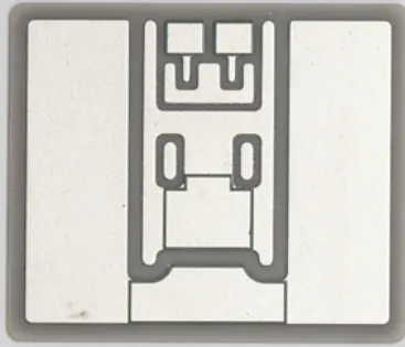
hello guys ! ! , You may or may not have the experience of printing your own custom PCB. There are many ways to follow in order to make a PCB. The usual way to print a circuit is to apply a pattern (circuit) Etching unwanted copper on a copper wrap plate. But if we can make our own copper plates, there\'s a lot of creative things that can be executed. So in this instructable, I will show you a way to make a custom PCB on any suitable surface. Any surface wants to make this possible. To weld things on the surface that keeps the copper layer, the copper layer should remain at a higher temperature of about 270 degrees Celsius. Materials such as plastic will not be made. I chose the glass in this demo. Because it can maintain the required temperature, and it is also great to make a transparent PCB. So let\'s start. . . . There are many technologies for making PCB. These technologies are different from the methods used for transmission modes (Circuit design). You can simply draw the circuit on copper with a permanent manufacturer. But this gives an untidy output. Or you can use the toner transfer method. In this note I will show you how to transfer the circuit to the copper plate using UV curing shielding. UV curing shielding provides ultra-fine output even if the track width is small. Even in the mass production of PCB. UV curing etching resistance light is a thin layer that becomes hard when exposed to UV light. This anti-light is laid on the copper plate and exposed to UV light by an opaque film consisting of circuit images. By the way, the circuit pattern is solidified on the anti-film. By applying developers, uncured films can be removed and circuits ready for etching can be obtained. Don\'t get confused with the word developer, it\'s just a low basic solution like baking soda that can remove uncured UV rays. There are two types of UV-resistant films, positive and negative. When the developer adds, the exposed part of the photo anti-photo remains undissolved while the rest dissolves. And vice versa. I used a negative in this structure. As mentioned above, we need to design the circuit into a transparent piece. This can be done by printing the design onto OHP paper. But first, we have to design the circuit. There are many platforms for designing circuits. Personally, I used an online circuit design software called \"EASY eda. It\'s easy to learn, free, and easy to find components. You may get familiar with it through some tutorials. Make a schematic diagram of your circuit first. Then model the PCB layout. After using the automatic wiring tool, the path of the circuit is defeated. This may sound a bit complicated for beginners. But with some tutorials, you\'re fine. There are a lot of unnecessary text and component diagrams in the design. We only need tracks and mats for our purposes. So after you meet the design, isolate the path from the pad layer in the layer tray and export the monochrome image as PNG. We use negative type photo anti-light, which means we need to expose the anti-light to light if we need to keep copper. There, the \"white on black\" option must be used in the export dialog box. This means it keeps the track and Mat White on a black background. White means that the OHP paper remains transparent after printing. So far, we have designed and exported the image. The purpose of OHP printing is to make a mask that blocks UV exposure against light in unwanted areas. To do this, the black part of the OHP print should block the light perfectly. If not, the light will leak out of them. A layer of print does not stop the light perfectly. Therefore, in order to maintain stability, 3 prints are aligned and placed together. As I mentioned above, I am going to make a copper that is placed on the glass. To do this, my plan is to stick copper foil on the glass. In the final stage, we have to remove unwanted copper by dissolving it with iron chloride. Choosing thick copper foil will cost the process more time. The thickness is about 0. Perfect 05mm. To prepare the glass, we must first clean the glass and copper foil with rubbing alcohol. If not, the copper will stick to the glass. After cleaning, apply the right amount of glue on the glass and apply it on the glass. Then put the copper foil and press it hard. Make sure there are no bubbles between glass and copper foil. Remove excess glue by squeezing copper foil. Let it be treated well. First, cut off the parts of the required size. Both sides of the photo anti-photo are covered with two transparent covers. The photo-resistant material is sticky. When the lid is removed, it can easily stick to the copper plate. Like I said, the resistance movie has two covers. We have to remove the lid in order to paste the anti-photo. To do this, we can paste two pieces of transparent tape on the top and bottom of the anti-film. Remove the cover by tearing through the tape. Then carefully place the uncovered side on the copper. To stick them all together, gently press the photo against photo. Make sure there are no bubbles between the anti-photo film and copper. After applying the photo anti now, we have to set it up now. Print out the OHP we did before. Put it on the copper plate. Please make sure the print location is correct. If not, the entire print may be mirrored. A piece of glass is placed after that to ensure that the OHP print is kept tight with the copper plate. I added two clips to keep the settings stable. It\'s time to be exposed to light. Now we have to set the exposure. You are free to use artificial UV sources. Bright sunlight is a good source of UV rays. The work can be done in about 5 minutes exposed to the sun. Ensure that the entire setup is stable during exposure. This clip does a good job. After 5- Remove the device from the bright sun for 7 minutes and remove everything. You should be able to see a little bit that the print on the resist print is cured. It is displayed in the image. There is also a cover on the top of the resist sheet. To develop it. We must also remove it. With the help of transparent tape, remove the cover again. Take some spare soda and make a solution with it. Any basic solution will affect his work. If you can\'t find the support soda, rinse powder can also do the job perfectly. In any case, in the developer ( Backing soda/washing powder solution) Dip the board and leave some time. Then take it out and wash it gently. You must be able to see that the unexposed parts are being washed away. Repeat the process until all unexposed parts are washed away. Finally, you will get a copper plate with curing resistance. Track. It\'s time for etching. . . Take a certain amount of iron chloride powder, dissolve in about 150 ml of the water, the solution must be dark. If no more iron chloride is added. After making the solution, dip the copper plate into the solution. Shake the circuit board frequently to effectively etching. About 10- After 15 minutes, all unwanted copper may be removed. The anti-resist on the copper path can be removed with some acetone or warm water. So what now,,. Making a PCB on Glass may not have any electrical advantage. These types of circuits can be used in many projects related to transparency. The led settings on a circuit like this might be great. This technology opens the way for many creative things. We are able to make PCB even on the surface. Instead of glass, kapton tape is able to make flexible circuits. I\'ll just stop here. I think you learned something new. . . . . .
Thank you for your attention. Please kindly describe your question first, or please send your inquiry to our email sales@rocket-pcb.com, and we will reply to you ASAP. Welcome, what can I help you?
We are here to help you! Please be sure to leave your contact details so that we can better assist you. Or click on the Skype button below to quickly communicate with us.