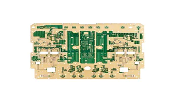
Presumably PCB laminate problem puzzled people for a long time, and engineers to discuss for a long time, to write this article.
Here small make up Rocket PCB factory name part of PCB laminate common problems and relevant solutions.
If PCB laminate such common problems, should develop a standard, have this problem after can suit the remedy to the case.
1.
Flow to scientific and reasonable this involved are many, such as high pressure/low pressure, input/output, strong/weak data signals, high frequency/low frequency and so on.
Their flow is the most reasonable should be linear, should not be mutual fusion.
It follows the principle is to eliminate dry scratching each other.
The flow of more appropriate is linear, but difficult to achieve.
The flow of the wrong is circular, thankfully and isolated this operation.
If specifically for dc, low pressure
PCB circuit board design requirements can be lower.
So the so-called 'scientific' is only relative.
2.
Power filter/decoupling capacitor rational layout of PCB circuit board layout for the appearance and properties of the whole circuit board, etc, are the key.
Only part of the power filter/decoupling capacitor will draw in the schematic diagram, but did not explicitly pointed out where they are received.
I think the capacitance is for switching devices or other needed parts of the filter/decoupling set, the position of the capacitor should be on those components, isolation distance you can't find the effect.
When we scientifically power filtering/decoupling capacitor, the ground of the common problem is no longer looks outstanding.
You can try!
PCB PCB/PCB 3.
The importance of ground is better choice ground must I don't need to say more.
Countless professionals to the discussion of it, usually require standard common point ground.
Multiple ground such as forward amplifier should meet with main together again after and so on.
But in real life, because of restricted by all kinds of difficult to completely achieve.
But we can't ignore, should make every effort to follow the principle.
The common problems in the actual situation is very flexible, different people have different solutions.
If you can specifically targeted at specific PCB circuit boards to describe is very easy to understand.
4.
Lines to choose reasonable call all circuit boards, lines, of course, it is important to drop!
The line conditions allow, as far as possible do some wide.
High pressure and high frequency line should be tactful, chamfering cannot appear sharper.
On a bend should not show 90 °, ground to wide as possible.
Want to solve the problem of ground point, a better approach is to a large area of copper clad.
If there's a better way to trouble in the comments section, leave a message, I also study more learning hee hee.
The problem of PCB circuit board with design and circuit board processing is inseparable.
For example some problems in post-production, when is likely to be caused by the PCB circuit board design.
Such as excessive line hole, substandard sink copper process is easily hide a lot of potential safety hazard and so on.
From the above questions we can draw a conclusion that in the PCB circuit board design should be as much as possible to reduce the hole thread.
If the same number of parallel lines, density is big, can together when welding.
As a result, production welding level decides the size of the linear density.
Solder joint spacing is too small, the difficulty of manual welding increases a lot at this moment the only way to solve welding quality -
—
Reduce the working efficiency.
Otherwise after problems will be more and more, also more and more difficult.
The level and efficiency of welding personnel the most narrow spacing determines the solder joints.
When the welding plate hole size is too small, or crossed the line for artificial drilling difficulty is increased.
When the size of the welding plate and borehole size does not match, it's a bolt from the blue for CNC drilling, welding plate is C word shape easily.
If the circumstances are serious bonding pad will be drill out.
If the cord is too thin, and on a large scale without copper wiring area, there are likely to be uneven corrosion phenomenon.
When after corrosion not wiring area, corrosion is likely to be excessively fine wires.
Sometimes look line is broken but didn't break, a little bit more serious it will break.
Therefore, copper set apply not only to expand ground area.
The above is purely personal point of view, if you have anything else to add in the comments below message, we make progress together!
Competitiveness policy of Rocket PCB Solution Ltd. is about existing clusters as a platform for upgrading microeconomic fundamentals, where structural policies aim to change the industrial composition of an economy more directly.
Click Rocket PCB for super quality from one of the state's premier producers.
As consumers get more and better information regarding how to compare various products and companies, it is critical to compete on the price and value of pcb making service.