AI technology drives surge in demand for high density interconnect PCB: servers and storage devices lead a new growth cycle for the PCB industry
PRODUCTS
PCB impedance board four elements
by:Rocket PCB
2020-07-19
Board PCB impedance is defined as: a good laminated structure can act as a control of the printed circuit board characteristic impedance, its line can be easily controlled and predictable transmission line structures called impedance board.
Now we know what the PCB impedance board is that you know about some elements of PCB impedance board?
On a printed circuit board, printed circuit board, characteristic impedance control characteristic impedance of the conductor is an important index for circuit design, especially in high frequency circuit PCB circuit board design, the characteristic impedance of the conductor must be considered and the device or whether the characteristic impedance of the signal required is consistent, whether the match.
2, printed circuit board impedance characteristics according to the signal transmission theory, the signal is a function of time and distance variables, therefore the signal on the attachment of each part are likely to change.
So sure the attachment of ac impedance, namely the ratio of the change of the change of the voltage and current for the characteristic impedance of the transmission line, the characteristic impedance of a transmission line is only associated with the characteristics of signal connection itself.
In the actual circuit, wire itself and the distribution of resistance value is less than the system impedance, especially in high frequency circuit, the impedance of the impedance characteristics of PCB board mainly depends on attachment of unit distributed capacitance and inductance of distribution impedance.
Ideal transmission line characteristic impedance depends only on the attachment distribution of unit distributed capacitance and inductance.
Three/circuit boards, printed circuit board PCB PCB impedance control circuit board of the conductor will have a variety of signal transmission, when the transmission rate and to raise its must raise its frequency, if the line itself due to factors such as etching, laminated thickness, wire width is different, will cause the change of the impedance value, make the signal distortion.
In high-speed circuit board on the conductor, the impedance value should be controlled within a certain range, known as 'impedance control'.
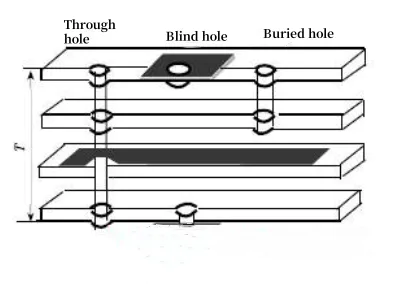
Factors that affect the impedance of the PCB circuit boards go line mainly have the width of the copper wire, copper wire thickness, the thickness of the dielectric constant and dielectric medium, the thickness of the bonding pad, the path of the ground, line the perimeter of the walk the line.
So when designing PCB must to control the impedance of the circuit boards go line, to avoid possible signal reflection and other electromagnetic interference and signal integrity problems, can guarantee the stability of PCB's actual use.
Microstrip line and the PCB strip line impedance calculation method can be reference to the corresponding empirical formula.
Four, printed circuit board of impedance matching in PCB circuit board, if there are signals, hope by the power of the end, in the case of the minimum energy loss, can smoothly delivered to the receiver, and receiver to be absorbed completely without any reflection.
To achieve this transfer, the line must be made the internal impedance and the impedance is equal to is called 'impedance matching.
In the design of high-speed PCB circuit, impedance matching is one of the elements of design.
The impedance values have absolute relationship with linear way.
For example, is walking in the surface layer, or inner layer, the distance from the power source of the reference layer or stratum, line width, PCB material etc all can affect walk line characteristic impedance values.
That is to say, after the wiring to determine the impedance value, at the same time different PCB manufacturers to produce characteristic impedance has little difference.
General simulation software will be used by circuit model or mathematical algorithm limits without considering some impedance discontinuity wiring situation, this time on the schematic diagram can set aside some termination, such as series resistance, go to mitigate the effect of line impedance discontinuity.
As far as possible when truly fundamental solution to the problem or wiring pay attention to avoid the happening of impedance discontinuity.
The above is the Rocket's small make up to you on the impedance of the PCB circuit board of the four elements (
Impedance control printed circuit boards, PCB characteristic impedance control, impedance characteristics of printed circuit boards, PCB impedance matching, etc. )
, hope to be of help.
Rocket PCB Solution Ltd. have now decided to extend our company in other countries.
Rocket PCB Solution Ltd. will accomplish this by exceeding the expectations of our customers while conserving resources and preserving the quality of the environment.
Depending on the scale of the service, Rocket PCB Solution Ltd. might also need to hire and manage an overseas workforce and comply with regulatory requirements.
pcb manufacturing services pcb making service quality is more important because some how it affects to our pcb manufacturing services. So grab good quality .
Through our distribution and marketing competencies, Rocket PCB Solution Ltd. provides creative, customized, solutions for our customers. As a result, we achieve superior profit growth as the pcb making service company of choice.
Custom message
Related Products