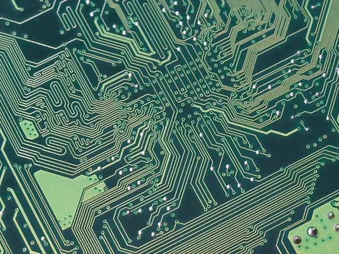
A bore, preface without copper also called impassability belong to PCB functional issues, with the development of science and technology (PCB precision
Aspect ratio)
Request is also more and more high, it not only brings to the PCB maker of trouble (
The contradiction between cost and quality)
, and buried a serious hidden dangers for the quality of the downstream customers!
Rocket
PCB manufacturer below small make up and everyone to look at together, hope to related colleagues some enlightenment and help!
2, 1 hole without classification and characteristics of copper, caused by PCB hole inside burr hole, as a result of drilling hole wall smooth and no burrs holes of copper, plating copper is not symmetrical.
Once the customer debugging electricity hole copper thin place could burn caused by open circuit PCB circuit boards via unreasonable result.
2, PCB electric copper thin hole without copper: (
1)
PCB whole board electrical copper thin hole without copper: copper sheet and copper electrode layer is very thin, with a figure handle most micro corrosion hole after the middle plate before electricity that is been to erode, figure after electricity by electric layer encase figure;
(
2)
Hole plate electric copper thin hole without copper: table electric copper layer is normal, hole plate electrode layer from the orifice to fracture showed a trend of decreasing icicles, and generally in a hole in the middle part of the fracture, fracture in the copper layer left right better uniformity and symmetry, figure layer encase figure electricity electricity after fracture.
PCB/PCB 3, PTH hole without copper: table electric copper layer is normal, hole plate electrode layer from the orifice to fracture distribution is more homogeneous, the chart layer encase figure electricity electricity after fracture.
Bad hole: (
1)
Copper repair bad hole: table electric copper layer is normal, hole electric copper layer no icicles trend, irregular fracture place, may appear in the hole may also occur in the middle, will often present as well as the rough bumps on the hole wall, map layer encase figure electricity electricity after fracture.
(
2)
Electric corrosion maintenance with hole: copper layer uniform normal, hole electric copper layer no icicles trend, irregular fracture place, may appear in the hole may also occur in the middle, will often present as well as the rough bumps on the hole wall, electric diagram layer in the fracture place to encase plate electrode layer.
4, jack no copper: PCB circuit board figure after etching, there is a clear material card plug in the hole, most of the hole wall is corrosion, electric diagram layer in the fracture place to encase plate electrode layer.
5, repair bad hole (
1)
Copper repair bad hole: watch PCB circuit board copper electrical layer, electric hole copper layer no icicles trend, irregular fracture place, may appear in the hole may also occur in the middle, will often present as well as the rough bumps on the hole wall, map layer encase figure electricity electricity after fracture.
(
2)
Corrosion maintenance with hole: watch PCB circuit board copper electrical layer, electric hole copper layer no icicles trend, irregular fracture place, may appear in the hole may also occur in the middle, will often present as well as the rough bumps on the hole wall, electric diagram layer in the fracture place to encase plate electrode layer.
6, electricity hole without copper, electric diagram layer in the fracture place to encase plate electrode layer - figure electric layer and PCB electric layer thickness, fracture has broken;
Electric diagram layer showed a trend of icicles until disappear, plate electrode layer more than figure continue a distance disconnect any electrical layer.
Three, improve direction 1, materials (
Plate, liquid medicine)
;
2, measurement,
Potions test, copper visual)
;
3, the environment (
Dirty, messy, mixed caused by variation)
;
4, method (
Parameters, procedures, processes and quality control)
;
5, operations,
On the lower, parameter setting, maintenance, exception handling,)
;
6, equipment (
Crown, feeder, heating pen, vibration and cheer, filter cycle)
。
If you have a
pcb manufacturing services business, be sure to choose a from Rocket PCB Solution Ltd.. After all, you need quality equipment in order to provide your customers with quality service.
Rocket PCB Solution Ltd., to be the world leader in products, services and solutions that enable and transform the way consumers and businesses gather, manage, distribute and communicate information.
When you choose to buy instead of
pcb manufacturing services, the money you save may allow you to buy multiple other necessities, more than you had initially planned on buying.
Visit Rocket PCB for the best in pcb manufacturing services pcb making service supplies and get the most cost effective for your pcb making service solution. Design and customization are also welcomed.