EasyEDA: a place to design your own printed circuit board, learning will always increase our thinking ability.
When learning a
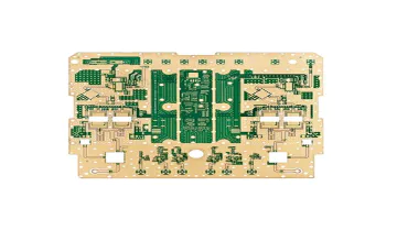
printed circuit board (PCB)
Design and then a technician will be very exciting.
PCB design, dealing with university projects, learning programming, and everything else will always add to one\'s interest.
Are you all looking for a platform where you can learn all of this and increase your technical content?
Then you are not far from your destination.
EasyEDA is a platform where you can test your skills, where you can learn new skills and even modify your skills.
This is a place to provide web-based EDA tools for electronic engineers, educators, students, manufacturers and enthusiasts.
You are welcome to use these tools for free and create your own online website
Based on the printed circuit board.
There is no need to install any software.
Just open EasyEDA in any standard that supports HTML5-
Conforms to the web browser.
Whether you\'re using Linux, Mac, or Windows;
Chrome, Firefox, IE, Opera, or Safari.
Chrome and Firefox are highly recommended.
With all the features you expect and need, EasyEDA can quickly and easily bring your design from concept to production.
If you wish to create a PCB, then in context, EasyEDA provides you with drawing tools, canvas tools, different cursor styles to enhance the appearance of the PCB.
It also gives a free demo of how to create embedded systems, Arduino projects, university projects, and more.
EasyEDA itself is a joint store for electronic products.
You can order PCB and other components simply by accessing the PCB order or part Order Label in easyeda. com.
You can create a new project simply by creating a new account on EasyEDA.
Even if you want to get pre-
Then you can also do PCB design close to this wonderful place.
You can share your project, and you can also view other people\'s projects.
Don\'t waste your time.
Just close to easyeda.
Com, create a new account and start your own PCB project.
Easyeda is the most valuable tool for electronics enthusiasts, engineers, amateurs and professionals. . .
Click here to read more in a given video tutorial, I have explained how to simulate or design a PCB for the schematic in simple steps.
Also, I have explained how to successfully order the first PCB from JLCPCB. JLCPCB (
Shenzhen jialichuang Electronic Technology Development Co. , Ltd. , Ltd. )
Is the largest
PCB prototype enterprise in China and
Technical manufacturer specializing in the production of fast PCB prototypes and small PCB
Mass production of PCB.
JLCPCB has more than 10 years experience in
PCB manufacturing, more than 200,000 customers at home and abroad, more than 8,000 PCB prototype online orders and a small amount of PCB production every day.
Step 1: Open EasyEDA online editor tool Step 2: Register or log in (
If you already have an account on EasyEDA)
Step 3: go to the file and open a new workspace window for the project Step 4: design the schematic using the tools and components available Step 5: Step 6: select all the required components and drag them to the workspace window: once you have successfully designed your schematic, then it\'s time to make it, this is step 7 of the Garber file: click the tab near the gear icon in the top window bar, and then click option convert project to PCB Step 8: now, you can choose either the \"auto track\" option or the \"manual track\" option, and I would recommend using the Auto track option as it will automatically reroute all the wires and will definitely save you time.
Step 9: if there is any problem, please check your PCB tracking and then do manual tracking at this point.
Step 10: once you have successfully verified your tracking, it is time to make the GERBER file.
If you really want to see the prototype of the PCB, I mean what your PCB looks like, then you have to have the GERBER file.
Step 11: please click on the \"Gerber Output\" tab near the photo View icon in the top window bar and a new window will appear with an option \"download your Gerber File \", click on this option and save your Gerber file in the PC in the new folder.
Step 12: Open JLCPCB, click the Add Gerber File tab, and then select the file saved in the new folder in the previous step.
It takes some time to load the GERBER File, mainly depending on the file size and the speed of the Internet.
You will see your PCB prototype when finished.
Scroll down and select properties based on your board. .
Click here to read more pictures about my Arduino-based prototype PCB for PV charge control! ! ! !
I was in a hurry to weld.
The Pcb is excellent, strong in quality, strong and beautiful.
As they mentioned on the jlcpcb page, I recommend this service. com.
The price is very good.
100% guarantee quality or rebirth.
Good Delivery time: 3 days DHL.
Online purchase order
Technical support if someone responds.
About the design, you can use any platform that allows you to generate your Gerber files, and maybe in the next tutorial you\'ll do it from KiCAD, which eagle will use a few years ago, but now, I will try to use open source.
Refer to Jlcpcb. comEasyEDA.
Jlcpcb. comEasyEDA.