How Advanced PCB Manufacturing Is Powering the Next Wave of Electronics Innovation
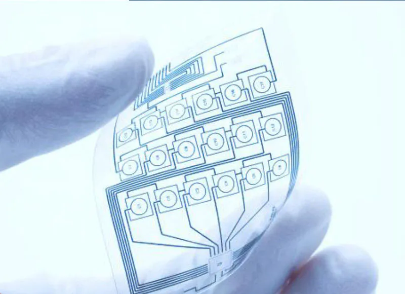
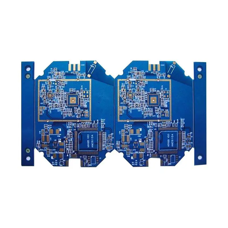
In today's electronics industry, innovation no longer depends only on powerful chips or smart software. Behind every reliable server, EV controller, medical device, or AI accelerator, there is a foundation that often goes unnoticed: the printed circuit board.
At Rocket-PCB, we work with customers every day who are pushing the limits of performance, reliability, and miniaturization. From high-speed communication equipment to high-power industrial systems, one thing is clear -- PCB technology has become a strategic component, not just a commodity.
In this article, we share several key trends shaping modern PCB manufacturing, and how companies can stay competitive in a rapidly evolving market.