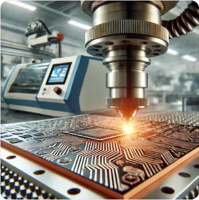
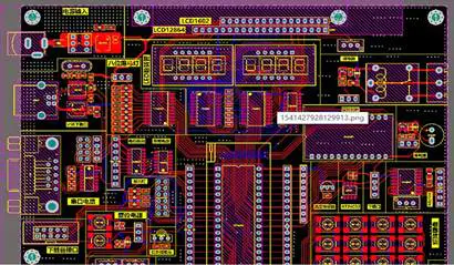
The most effective way to improve the density of
PCB circuit board is to reduce the number of hole, and the precise setting blind holes, buried hole.
Blind holes to define a: as opposed to a hole, hole is refers to the layers of all drill holes, blind holes are drill hole.
B: blind hole segmentation: blind hole (
BLINDHOLE)
Hole, buried BURIEDHOLE (
The outer not see)
;
C: to distinguish from the production process: blind hole drilling, before pressing and drilling hole is after pressing.
Dongguan circuit board factory, circuit board manufacturing method A: drill: (
1)
: select reference points: select hole (
The first drill with a hole in the)
The reference hole as a unit.
(
2)
: each blind hole drill with all needs to select a hole, the coordinates of the reference hole with its relative unit.
(
3)
What: note that the drill with which a few layer: the corresponding unit points figure and drill hole nozzle table must be noted, and the name should be consistent;
Cannot appear hole figure in ABC, and the front with 1 st, 2 nd said.
Note when laser hole and buried the inner hole set together, the two belt of drill hole on the same position, need to ask the guest the location of the mobile laser hole to ensure the electrical connection.
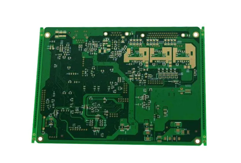
B: dongguan circuit board factory in the production of PNL technology hole edge: normal PCB multilayer circuit board: the inner hole;
(
1)
Gh: rivet, aoigh, after etgh are etched plate type (
2)
: the target hole (
Drilling gh)
The CCD: outer tao copper, x -
Ray machine: hit directly, and pay attention to the minimum of 11 inch long side.
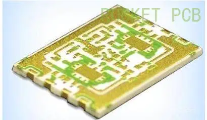
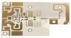
Blind buried orifice (
Printed circuit board)
PCB PCB of blind hole plate: all tooling holes are drilled, pay attention to the rivet gh;
Need to beer out, avoid the registration deviation.
(
Aoigh also for bei)
, the production of PNL edge need to drill the words used to distinguish between each panel.
Film modified: (
1)
: indicate the qualities of the positive and negative: general principles: mil thickness greater than 8 (
Not even the copper)
Go positive process;
Mil thickness less than 8 (
Not even the copper)
Negative process (
Sheet)
;
Thick line gap valley should be considered when big d/f of the copper thick, rather than the bottom copper thickness.
Do 5 mil blind hole ring, do not need to do 7 mil.
The lining of the blind hole corresponding to the independent pad should be retained.
Hole can not do without the ring hole.
Dongguan circuit board factory process: buried orifice plate with ordinary double-sided circuit board practice.
Blind hole plate, that is, one side is the outer: positive process: do single d/f, attention should be paid not roll fault plane (
Double bottom copper inconsistent)
;
D/f exposure, the copper surface covered with black tape, prevent the pervious to light.
For blind hole plate to do two or more electricity, electricity, finished product thickness of super thick extremely easily, so the figure electric pay attention to the control panel thick copper thick, indicate the scope of the copper plate thickness after etching.
After pressure plate with X-ray
Ray machine with multilayer circuit board with the target holes.
Negative process: according to the sheet,> < 12 mil even copper because its not the batteries in figure production, must be in gold production, water and water can't points gold surface current, so it can't make a single according to the requirements of the mi not dozen current or low current.
Such as positive process, often result in a single copper ultra thick thick, etching difficulties, the phenomenon of young line, so this kind of plate negative process.
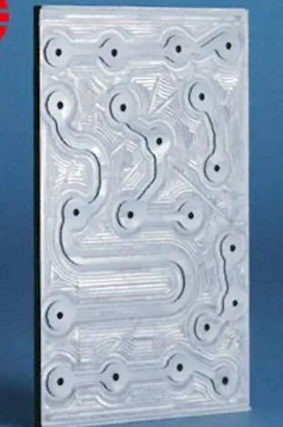
Hole, blind hole drilling in a different order, making the deviation inconsistent deformation, caused by blind hole plate is open with material for profes sional counterpoint and tube spacing control is difficult, therefore, only when cutting open horizontal or driving down a perfectly straight only material.
Should pay attention to such board andante process line with resin sealing hole first and then do so as not to cause great damage to the circuit.
pcb making service is an inevitable and critical part of being a manufacturer, and it's more complicated than just manufacturing products and serving customers.
Rocket PCB Solution Ltd.’s sole aim is to provide exquisite and unheard of features to the concept of producing technology.
pcb making service receives the updates through industry associations, internal legal counsel, regional associations and legal publications.