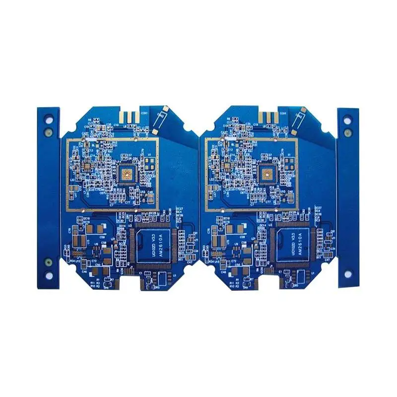
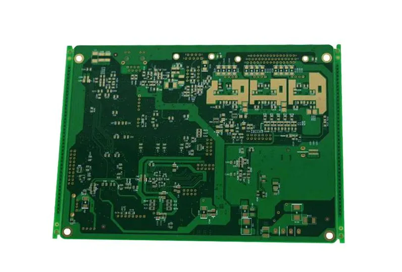
PCB applications and uses
From mobile phones to house appliances, electronics perform a huge aspect in the daily routine. In the heart of every electronic is actually a printed circuit board.


When PCB proofing by way of surface treatment, the surface treatment method has its unique characteristics, chemical silver, for example, its process is very simple, recommended to be used in lead-free soldering and SMT, especially for fine line effect is better, the most important thing is to use chemical silver surface treatment, will greatly reduce the overall cost, cost is low. By the Rocket PCB circuit below small make up for you introduce several kinds of common PCB proofing surface treatment. Hot air leveling (HASL Is often said that the spray tin) Tin is PCB proofing early treatment methods in common use. Now divided into tin with lead and lead-free tin. Advantages of spray tin: after the completion of the PCB, fully wetting on the surface of copper ( Completely covered before welding, tin) Mature, suitable for lead-free soldering process, lower cost, suitable for visual inspection and electric logging, also belong to one of high quality and reliable PCB proofing processing mode. Chemical nickel gold ( ENIG) Chemical nickel gold is application of a PCB proofing surface treatment technology, remember: nickel layer is nickel phosphorus alloy layer, on the basis of phosphorus content is divided into high phosphorus nickel and nickel phosphorus, applications are different, not to introduce the difference here. The advantages of chemical nickel gold: suitable for lead-free soldering; Surface is very smooth, suitable for SMT, suitable for electric test, switch contact design, suitable for aluminium wire binding, suitable for thick plate, stronger resistance to environmental attack. Plating nickel plating nickel gold is divided into 'hard' and 'soft gold', hard gold ( Such as: gold cobalt alloy) Commonly used in gold finger ( Contact connection design) , soft gold is pure gold. Gold plating nickel in the IC board ( For example, PBGA) Applied more, mainly applicable to gold wire and copper wire binding, but the IC load board suitable for electroplating, binding goldfinger areas need to be extra do conductive line out to plating. Advantages of electroplating nickel gold PCB proofing: contact switch design and gold wire binding; Nickel, palladium, ENEPIG) Nickel, palladium is now gradually began to start application in the field of PCB proofing, before more in semiconductor applications. Suitable for gold, aluminium wire binding. With the advantages of nickel and palladium PCB proofing: application on IC loading board, suitable for gold wire binding, aluminium wire binding. Suitable for lead-free soldering; Compared with the ENIG, no nickel corrosion ( Black plate) Problem; Cost is much cheaper than ENIG and electroless nickel gold, suitable for a variety of surface treatment technology and was on the board. In addition to the above PCB proofing processing ways, including chemical tin, tin this kind of chemical surface treatment applied to horizontal line production, also use, fine lines, processing of the project you when choosing PCB proofing surface treatment way, according to the actual situation, the characteristics of the contact way of surface treatment, budget, cost, also can choose appropriate PCB proofing spot wholesale products.
Quick Links
About Us
Contact Us
Tel:(+86) 158 9965 5195
Office:(+86) 755 23040566
E-mail:sales@sllpcb.com
Microsoft Teams:hank_168
WhatsApp:+86 186 0723 3179
Office Address:2207,Bid 4,He Gu Shan Hui Cheng,35#,Guang Tian Ro Yanluo street, Song Gang Town,518105 SHENZHEN, CHINA
Plant ADD: No 69, Lianfeng North Road, Xianxi Area, ChangAn Town, Dongguan, China.