Hello everyone, this is a note on \"how to make PCB at home\" without any special material.
As a student in electronic engineering, I try to make DIY projects that require simple electronic circuits and pcb. What is PCB?
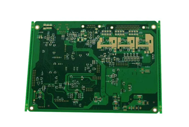
Printed circuit board (PCB)
Mechanical support and electrical connection of electronic components using conductive tracks, pads and other functions, from lamination to non-
Conductive substrate.
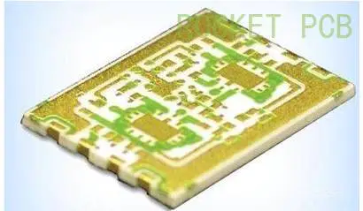
Pre-printed circuit board
Copper tracks designed on wires. The pre-
Defined tracks reduce wiring, thus reducing failures due to lost connections.
We need to simply place the assembly on the PCB and weld it.
There are three basic ways to make pcb1.
Method of iron on coated paper 2.
Manual circuit on PCB 3.
Laser cut edge etching.
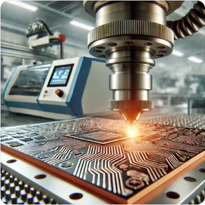
Since the laser method is the industrial method of manufacturing PCB, we will learn more about the first two methods of manufacturing PCB in China.
This is usually done by using the PCB layout software to convert the schematic of the circuit into a PCB layout.
There are many open source packages for PCB layout creation and design.
Here\'s a list of some for you. start: 1.
Cadsoft Eagle month.
I designed my circuit schematic in Cadsoft Eagle.
Note: In Eagle: File> Export> image, be sure to set DPIG to 1200 some old clothes for better quality.
To start making the PCB, consider using the simple item touch switch of ic555 and printing it out of the PCB layout using a laser printer and A4 photo paper/sheet paper.
Please keep in mind the following: cut the copper plate according to the size of the layout.
Rub the copper side of the PCB using steel wool or grinding sponge scrub.
This will remove the top oxide layer and the photo-resistant layer of copper.
The sanding surface allows the image to stick to the better Method 1: ironing method on the smooth paper: Transfer the printed image from the photo paper to the board.
Make sure to flip the top level horizontally.
Place the copper face of the circuit board on the printed surface.
Make sure the board is aligned correctly along the boundaries of the print layout.
Tape along both sides of the boardcopper side.
This will help to maintain the position of the board and print layout.
Method 2: circuit using permanent marker pen: use the circuit image reference printed on the smooth paper, draw the basic sketch on the copper plate with a pencil first, and then draw it with permanent black marker pen.
Note: Do not contact the copper plate directly because of the ironing, because it is very hot.
After ironing, put the plate in Luke\'s warm water for about 10 minutes.
The paper will dissolve gently and remove the paper.
Remove the paper at low angles and marks.
In some cases, some tracks faint when the paper is taken out.
See the figure Black line track in the white box is light in color, so we can use the black mark for dark lighting the track as shown in the picture. You need to be very careful and cautious or plastic gloves when performing this step
Place some newspapers so that the etching solution does not break the floor. 1)
Take a plastic box and fill it with some water. 2)Dissolve 2-
Add a tea spoon of trichloride iron in the water. 3)
Immerse the PCB in an etching solution (
Iron Chloride solution)
About 30 minutes. 4)
FeCr 3 reacts with unshielded copper and removes unwanted copper from the PCB. 5)
This process is called etching.
Remove the PCB using pliers and check if the entire unshielded area has been etched.
If there is no etching, please keep it for a while in the solution.
Gently move the plastic box back and forth so that the etching solution reacts with the exposed copper to form iron and copper chloride. After every 2-
3 minutes to check if all copper is etched.
Do not touch the etching solution directly. In the picture, we can see that copper is slowly etched.
The etching solution is toxic to fish and other aquatic organisms.
Don\'t pour it in the sink when you\'re done.
It is illegal to do so and may damage your pipe.
Dilute the etching solution and then process the solution.
The figure shows the PCB of the two circuits made using print output and marking.
A few drops of thin material (
Nail Polish stain remover works well)
A pinch of cotton wool can completely remove the toner and restore the surface of the copper.
Rinse and dry carefully with clean cloth or kitchen paper.
Trim to the final size with sandpaper and refine the edges.
Acetone helps the oil paper stick to rough paper.
All components and PCB are ready for drilling and welding. Cheer! ! 1.
The iron method on coated paper is an effective way to make pcb in China.
If done carefully, each track can be printed perfectly. 2.
The manual circuit on the PCB is limited to our artistic skills.
It is easy to make simple circuits with this method, but it is best for complex pcb iron on smooth paper.
Thank you for sticking to this step.
I only need a few seconds.
You can visit my websitewww. blogtheorem.
I have published interesting articles about science, engineering and technology here.