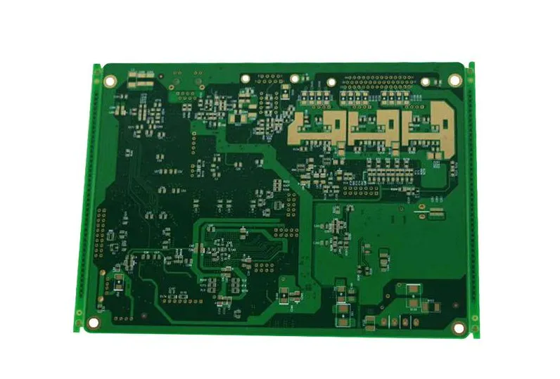
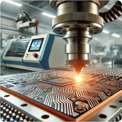
Actually red glue process can be improved after welding, the efficiency of this process the one who is, as long as do all know PCB SMT processing, let's first take a look at the red glue process is what to do.
Red glue process, as the name implies, is to use red glue for patches, when opening the stencil is not open components welding plate position, but in the middle of the element position open a slot, brush on red glue, and then on SMT type element, this element is red tape on the PCB, with plug-in of material after the tin stove, component soldering pad is meeting.
Glue process schematic diagram and one red red glue process there are some problems: can be seen from the figure 1, the red glue will be a certain thickness, the elements in the process of the hardened high top, it'll be easier for components of welding plate and
PCB circuit boards welding plate clearance, once there is gap, is easy to appear on the tin bad form virtual welding;
Another red glue will become very hard after the tin stove, if need to replace components for repair work and so on will be very troublesome;
And red glue in a tin stove temperature easy to take off the parts, especially the IC are more likely to happen.
Red glue process diagram today Rocket PCB factory small make up to introduce this method can avoid these problems of red glue process, take a few picture first.
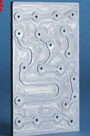
Figure 2 a fixture of figure 2 fixture has some holes and slot: the location of the hole is needed after welding, the pin of the plug-in can wear out from inside the hole, put the fixture on the tin stove top, only these hole location can access to the solder;
Groove corresponding is after the PCB SMT components, components of dig big points, components soon small dots, so good patch components of PCB can flat on top of fixture.
PCB SMT a fixture of figure 3 is applicable for the fixture in figure 3 each PCB PCB circuit boards with two size bigger chip, a nearly square, a rectangle, with the two chips and groove matching in figure 2, will know that a good patch components of PCB fixture on how flat.
Suitable fixture of PCB circuit board figure four fixtures into have SMT PCB base plate is a good patch components by figure 4 on fixture after the appearance of the floor, can very clearly see the exposed are plug-in components of welding plate hole, pin of components from the bonding pad via through to the surface into the tin stove, whether can the all plug-in material welding good?
Fixture in has SMT PCB bottom figure five fixtures in have patch on the back to look at the back of PCB, I don't need to explain all know it can be easily for the plug-in.
This method can let the welding efficiency significantly increased after, but the plugin is near the welding plate not have other tiles, if too close to the bonding pad can't opening, behind the need to manually repair welding.
Fixture in have patch on the back of the PCB circuit boards
Rocket PCB Solution Ltd. is dedicated to servicing our customers with a wide array of high-quality service and products.
As a global pcb making service company, we take on some of the world’s biggest pcb making service challenges. Rocket PCB Solution Ltd. have a whole series of
pcb manufacturing services pcb making service that can solve your pcb making service problem in an effective manner. Check it at Rocket PCB .
The only cardinal rule with adding animation is to keep high-quality on pcb making service.