When you are going to design your own PCB, you need to draw holes, pads and wires for your circuit.
Then you send the painting to the manufacturer or you etching it yourself.
You need to know what circuit you want to build before you start drawing wires and other things.
So you need to find or design a schematic for your circuit.
You need a PCB design software.
Then you can start the process.
First draw the schematic diagram into the software of your choice.
Here we will use the free PCB design tool EasyEDA to show how to design the board using the sample PCB of the voice modulator circuit.
Voice modulation circuit, we are ready to make a voice modulation circuit, usingdesigned PCB.
This is an interesting project designed mainly to change or change the sound.
Generally speaking, when we talk in a microphone, we hear the same sound.
But in this project, when we talk with a microphone, we hear a few different sounds, just like the robot is talking.
Circuit diagram and description: LM358 op-is used in this voice modulator circuit-
Audio amplifier IC and LM386.
Users can drive this circuit using 3 to 9 volts.
In this circuit, we use the band-
Through filter circuit made using op-
Amp IC and R10 pot for changing the gain of the microphone preamp circuit.
IC LM386 for amplification of speech modulator signals.
At the time of output, we have two options to listen to the modulated sound: the speaker and 3.
Headphone 5mm jack.
Pot 5 is used for volume control.
Jumper J2 is used for the gain of the audio amplifier.
You can access the entire circuit and PCB layout of this voice modulator circuit through the following link: Step 1 the user needs to open the EasyEDA website and then register when used for the first time, otherwise log in with your credentials.
Create a new project, click New schematic \"(blue circle)
Or the user can directly perform the PCB layout by clicking on the new PCB (red circle)
As shown in.
Now you will see the schematic window where users can select the required components from the EasyEDA library in the panel on the left side of the site.
Users can see symbols such as resistance, capacitance, inductance, power, etc.
And it is possible to move the cursor to where you want to place the component by clicking any item on the schematic, and finally clicking again to place the component.
If you want to get more components then he/she can use more library search options on the left side of the screen.
Then, you will get another window for selecting components with categories and search options.
This is how the user gets the required components.
After getting all the components, the next part is to connect the components to each other, and EasyEDA has a window of cabling tools.
In this tool, by selecting wire, we can connect components by clicking on the start point and then the end point.
As you can see, we have started drawing the voice modulator circuit as shown in the above figure.
Here we have finished the drawing and now is the time to write the text on the schematic by selecting the \"T\" option from the drawing tool.
Here we have shown this in the red circle in a given picture.
Now you need to connect the Vcc and ground to the circuit.
To do this, you can select power and ground from the EasyEDA library on the left
Hand side of the screen.
Finally, you can save the schematic by selecting the blue folder icon as shown below and clicking save, and then save the schematic by giving the schematic the appropriate name.
Now the circuit is ready for PCB layout conversion.
For the PCB layout, the user needs to move the cursor over the manufacturing label as shown in the following figure.
Here you will see converting the project to a PCB and you will redirect to the PCB layout window by clicking on it.
Now you need to place all the components in the desired location and save the layout as we save the schematic.
You can manually route the circuit with the help of PCB tools, or there is automatic wiring function in EasyEDA (red circled)
, It will automatically route all connections for you.
In the picture given below, the user can set the track width, Gap (Trace clearance)
, Automatically route the layers and other things before, and then click Run \".
Then you will see the automatic
The route will start and will be completed in a few seconds.
Then you will see the result given.
Now you can pour the copper on the top and bottom and select the top layer by selecting the copper on the PCB toolsTop copper area (
See the black circle in the picture below)
And then the bottom layer.
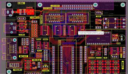
Finally, we have the PCB layout ready.
After drawing the circuit board, it is time to design the PCB for manufacturing.
This basically means you need to check if there is an error with your motherboard and convert your motherboard layout to a Gerber file.
Then, choose a cheap
PCB manufacturer to make your board.
We manufacture sample PCB using EasyEDA
PCB manufacturing service.
After completing the PCB design, you can click on the icon above to make the output, it will take you to the PCB order page, you can download or view the gerber files of the PCB and send them to any manufacturer, it\'s much easier (and cheaper)
Order directly at EasyEDA.
You can order this PCB directly or download the Gerber file using this link.
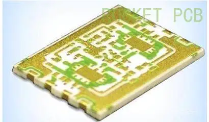
I ordered 5 voice modulator pcb from EasyEDA and they arrived at my door two weeks later.
After checking, I can see that the pcb is well made and can\'t find the defect on any piece of board.
Pcb works very well in electricity.
If you want, you can clone my voice modulator schematic and PCB here and start designing your own PCB board.