Electronic Products, printed circuit boards or printed circuit boards are used for mechanical support of electronic components whose connecting leads are welded on copper pads in surface-mounted applications, or weld component leads through oblique holes and copper pads on the circuit board
Hole application.
A board design may have all passed-
Hole Assembly on the top or side of the Assembly, straight through mixing
Mounting holes and surfaces on top only, mixed
Hole and surface mounting assembly at the top and surface mounting assembly at the bottom or on the circuit side, or surface mounting assembly at the top and bottom of the plate.
The board is also used to electrically connect the leads required for each assembly using a conductive copper trace.
Component pads and connection traces are laminated from non-
Conductive substrate.
Printed circuit boards are designed to be single sided, only with copper pads and traces on one side of the board, copper pads on both sides, traces on the top and bottom of the board, or multi-layer designs, copper pads and traces on the top and bottom of the board, the number of copper layers inside is variable, with traces and connections.
A single or double panel consists of a core dielectric material such as FR-
4 epoxy fiberglass, copper plated on one or both sides.
As part of the circuit board manufacturing process, this copper plating is etched to form actual copper pads and connection marks on the surface of the board.
The multi-layer board consists of many layers of dielectric material soaked with adhesive, which are used to separate the copper plating layer.
All of these layers are aligned under heat and pressure and then combined into a single board structure.
Using today\'s technology, it is possible to produce multiple layers of 48 or more layers.
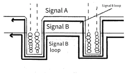
In a typical four-layer board design, internal layers are often used to provide power and ground connections, such as 5v plane layers and ground plane layers that act as two internal layers, connect all other circuits and components at the top and bottom of the board.
Very complex circuit board designs may have a large number of layers to be connected for different voltage levels, ground connections, or for connecting many leads on ball grid array devices and other large integrated circuit packaging formats.
There are usually two kinds of materials used to build multi-layer boards. Pre-
Pre-dip is a thin layer of glass fiber
Dip with adhesive, usually in the form of paper.
Thickness 002 inch
The core material is similar to a very thin double panel because it has a dielectric material such as epoxy fiberglass, which usually deposits a layer of copper on each side.
Dielectric material of 030 thickness, with 1 ounce copper layer on each side.
In multi-layer board design, there are two ways to build the required number of layers. The core stack-
The Up method is an old technique that uses a central layer
A layer of core material on the top and a layer of pre-dip material on the bottom.
A combination of pre-
The Preg layer and the two core layers will be made into 4 layers. The film stack-
The Up method is a relatively new technology that takes the core material as the central layer, followed by the layer pre-
The pre-dip and copper materials piled up above and below form the final layer required for board design, a bit like a Dagwood build sandwich.
This method allows the manufacturer to flexibly combine the board layer thickness to meet the finished product thickness requirements by changing the number of pre-coated plates
Pre-dip each layer.
Once the material layer is completed, the entire pile is subjected to heat and pressure, resulting in pre-
Glue the core and pre-dip together
Combine the preg layer into one entity.
For most applications, the process of making a printed circuit board follows the following steps: the basic steps of making a printed circuit board: 1. Setup -
According to the Gerber document information provided by the purchase order, determine the process of meeting the material, process and requirements of the customer\'s circuit board design specifications. 2. Imaging -
The process of transferring the layer\'s Gerber file data to the etching anti-film placed on the conductive copper layer. 3. Etching -
The traditional exposure of copper and other areas not protected by etching protective film to chemicals that remove unprotected copper leaves protected copper pads and traces;
The newer process uses plasma/laser etching instead of chemical substances to remove copper material, allowing for finer line definitions. 4.
Multi-layer pressing
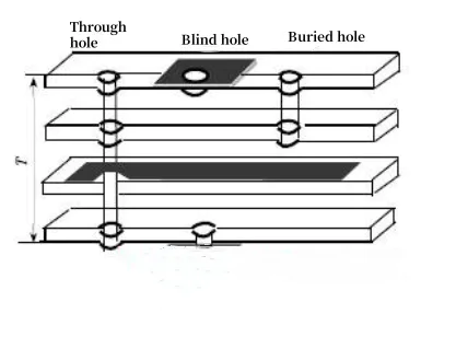
The process of aligning the conductive copper and the insulating dielectric layer and pressing it under heat to activate the adhesive in the dielectric layer to form a solid plate material. 5. Drilling -
The process of drilling all holes by application;
For holes that are not plated, a second drilling process is used.
Information about the location and size of the drill is included in the drill drawing file. 6. Plating -
The process of applying copper plating to pads, traces and drilling to be thoroughly plated;
The board is placed in a copper bath full of electricity. 7.
Second drilling
This is required when drilling through the copper area but the holes are not plated.
Avoid this process if possible, as it will increase the cost of the finished board. 8. Masking -
The process of applying protective shielding materials, welding masks on bare copper marks or on a thin layer of welded copper;
Welding masks prevent damage to the environment, provide insulation, prevent short circuit of welding, and protect traces between pads. 9. Finishing -
The process of applying a thin layer of solder to the pad area to prepare for the final wave soldering or reflow soldering process, which will take place at a later date after the assembly is placed. 10.
Silk screening
The process of applying the part name and the part profile mark to the board.
If the component is installed at the top and bottom, it can be applied only to the top or both sides. 11. Routing -
The process of separating multiple plates from a panel composed of the same plates;
This process also allows cutting gaps or slots into the board if required. 12.
Quality control-
Visual inspection of wooden boards;
It can also be the process of cross-checking the Wall quality of the penetrating hole on the multi-board
Slicing or other methods. 13.
Electrical test-
The process of checking the continuity or short circuit connection on the board by applying voltage between points on the board and determining whether a current occurs.
Depending on the complexity of the board, this process may require a specially designed test fixture and test program to be integrated with the electrical test system used by the board manufacturer.