English


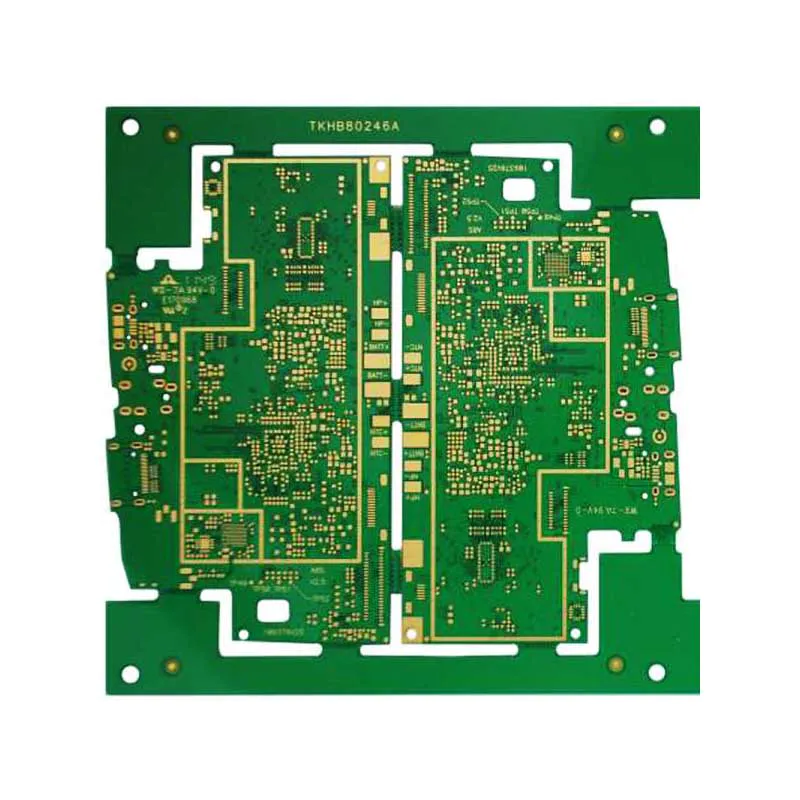
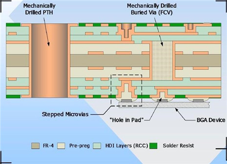
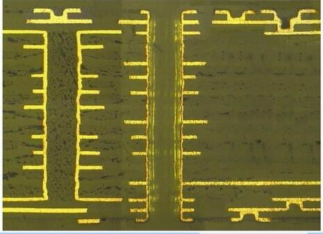
Compared with conventional PCBs, HDI PCB has a higher density per unit of the circuit. They use a combination of buried and blind holes, as well as micro-holes with a diameter of 0.006” or smaller micro vias.
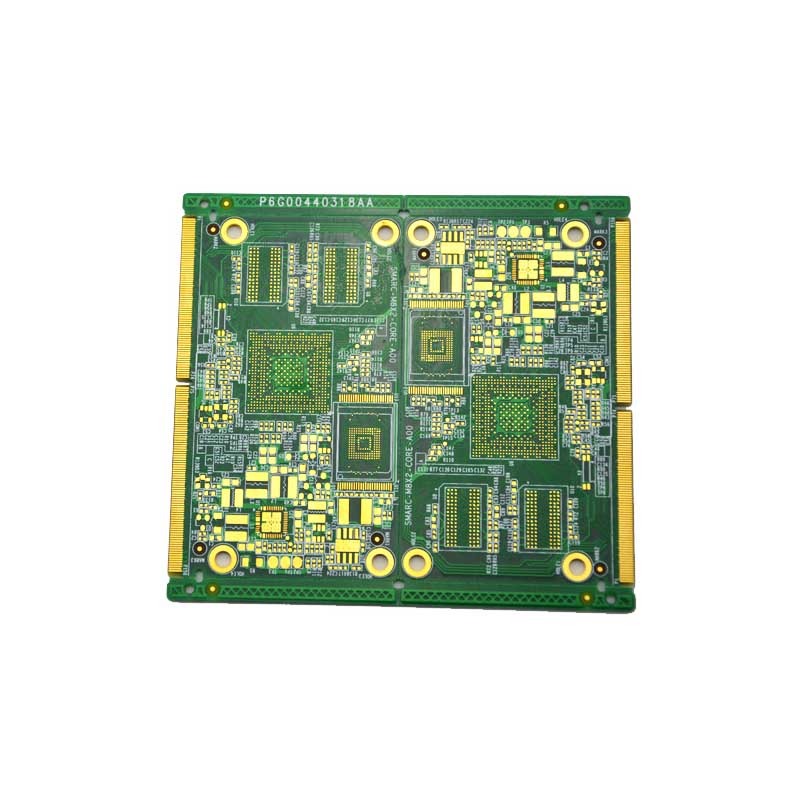
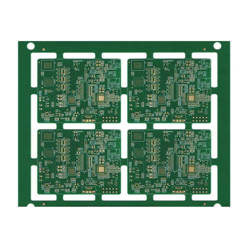
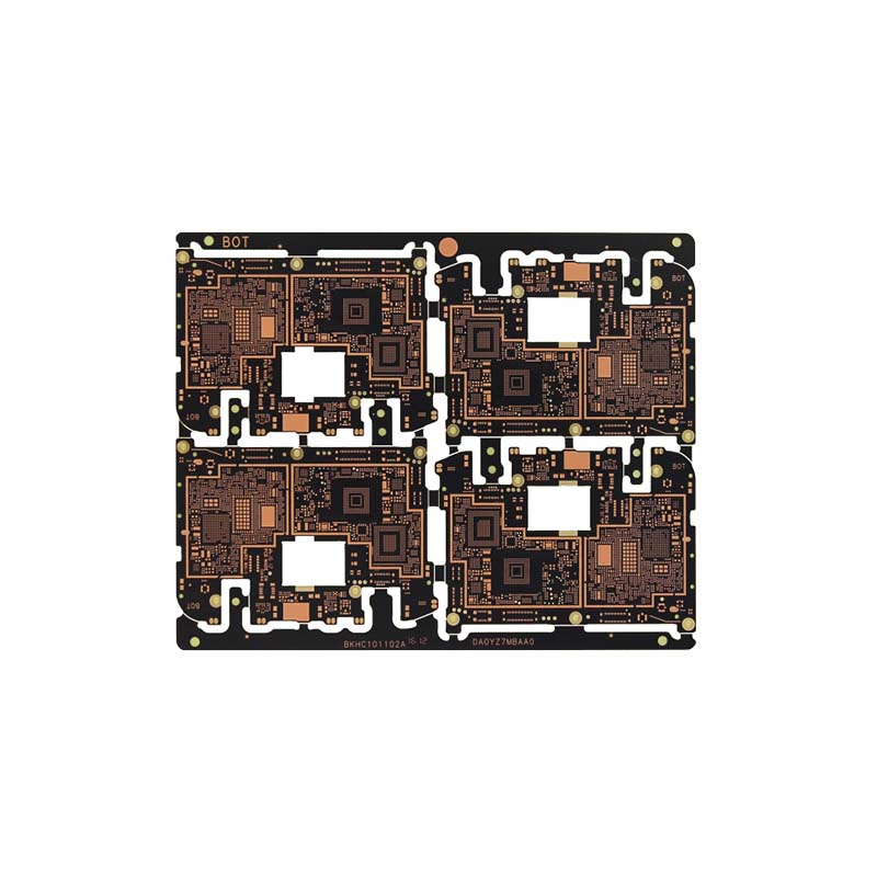
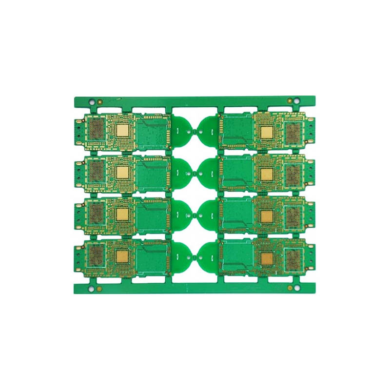
The strict tolerances involved in using HDI printed circuit boards mean that you need to work with experienced suppliers. Even small defects or layout accidents can lead to serious problems. As a leading supplier of HDI printed circuit boards, Rocket PCB offers top-notch circuit boards with a much higher circuit density than conventional PCBs.
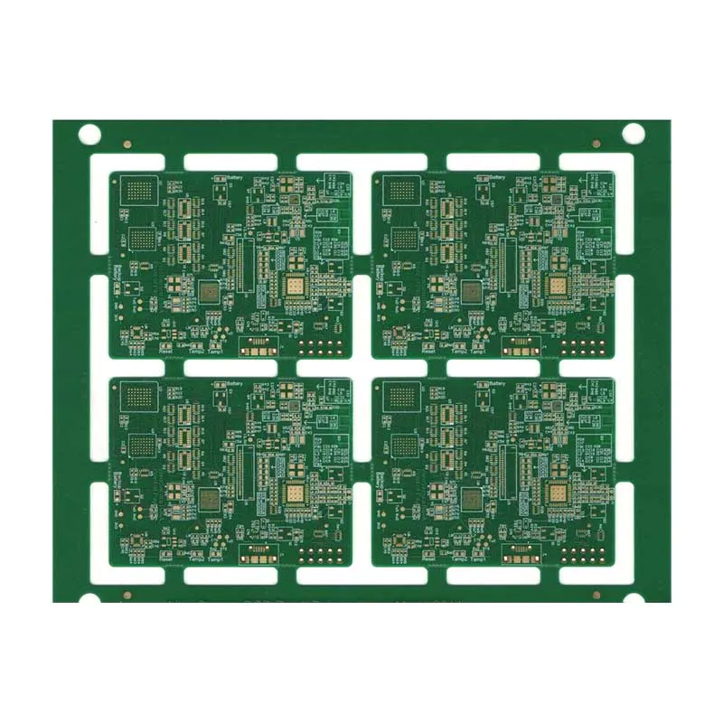
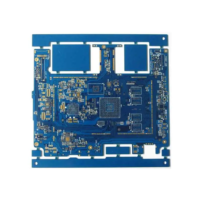
Want to know more product information? We will provide you with detailed pictures and detailed content of HDI PCB fabrication in the following section for your reference. Rocket PCB has a scientific and perfect procurement chain. To guarantee the quality from the source, we always adhere to the selection of high-quality materials to produce all kinds of printed circuit boards. They are highly safe that have passed the national compulsory certification. We provide a worry-free buying experience for customers. Rocket PCB has professional production workshops and great production technology. HDI PCB we produce, in line with the national quality inspection standards, has a reasonable structure, stable performance, good safety, and high reliability. It is also available in a wide range of types and specifications. Customers' diverse needs can be fully fulfilled.
| Items | Capability |
|---|---|
| Circuit Constructions | Single-Sided / Double-Sided / Multi-Layer / Flex / Rigid Flex |
| Material | FR-4 / Rogers / Arlon / Polymide / Aluminum / Kapt/etc |
| Copper weights | 0.5oz~10oz |
| Layer Count | 1-64 layers |
| Stack up | Control Dielectric/Control Impedance/TDR Testing |
| Surface finish | Lead-Free/HASL/ENIG/ENEPIG/Hard Gold/Wire Bonded Gold/Immersion Silver/OSP/selective osp |
| Vias | Blind-buried/via-in-pad/POFV/Filled-vias/epoxy resin filled vias |
| Advanced tech | Embedded /Laser drill/Multi-level cavity/Build-up HDI/Long-short staged gold finger/Hybrid/metal-core/press-fit |
| 1+n+1 | Yes |
| 1+1+n+1+1 | Yes |
| 2+n+2 | Yes |
| 3+n+3 | Yes |
| 4+n+4 | Yes |
| Any-layer | 12L |
| Laser孔径 max | 0.15mm |
| Laser孔径 min | 0.075mm |
| Laser盲孔厚径比 max | 0.8:1(Depth included copper thickness) |
| Laser盲孔电镀填孔 | Yes (laser via size 4-5mil, priority 4mil) |
| Laser盲孔树脂塞孔 | Yes |
| Stack via | 5step |
| Stagger via | 5step |
| Filling via dimple value 电镀填孔凹陷深度最大 | <=15um |
| Laser via capture pad size 外层laser PAD标准 (外层laser孔+两边ring) | 0.25mm |
| Laser via hole size Laser孔径标准 | 0.1mm |
| Laser via land pad size 对应内层PAD | 0.25mm |
| Minimum spacing between laser hole edge to laser hole edge (Same Net) laser孔边到Laser孔边最小间距 (同一网络) | 0.1mm |
Minimum spacing between laser hole edge to laser hole edge (Different Net) Laser孔边到Laser孔边最小间距 (不同网络) | 0.25mm |
| Max finished hole size for blind & buried via | 0.3mm (max) l(corresponding drilling tool size 16mil) |
| Minimum spacing between laser hole edge to buried drill hole edge (Same Net) Laser孔壁到埋孔孔壁最小间距 (同一网络) | 0.1mm |
| Minimum spacing between laser hole edge to buried drill hole edge (Different Net) Laser孔壁到埋孔孔壁最小间距 (不同网络) | 0.2mm |
| Minimum spacing between laser hole center to board edge (Inner layer) Laser孔中心到板边最小间距 (内层) | 0.35mm |
Minimum spacing between laser hole center to board edge (Outer layer) Stamped/Routed edge Laser孔中心到板边最小间距 (外层) | 0.3mm |
| Minimum spacing between through VIA hole edge to PADs (Outer layer) (Different Net) 通孔孔壁到外层PAD最小间距(不同网络) | 0.18mm |
| Min thickness to Internal layer 内层板最小厚度 | 0.05mm |
| Max. dielectric thickness 最大介质层厚度 | 0.1mm |
Min. dielectric thickness 最小介质层厚度 | 0.05mm |


Product Message
QUICK LINKS
CONTACT US
Office: (+86) 755 23040566
Tel: (+86) 158 9965 5195
E-mail: sales@rocket-pcb.com
Skype: Hans@Rocket-PCB
Whatsapp: 86 1589965 5195
Office Address: 301 Building/B, Huafeng Digital Technology Industrial Park, Chaoyang Ro, Yanchuan, Songgang,518105 Shenzhen, China.
Plant ADD.: No 69, Lianfeng North Road, Xianxi Area, ChangAn Town, Dongguan, China.