
Hot products
English


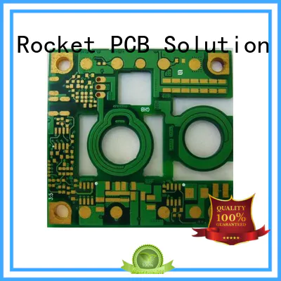
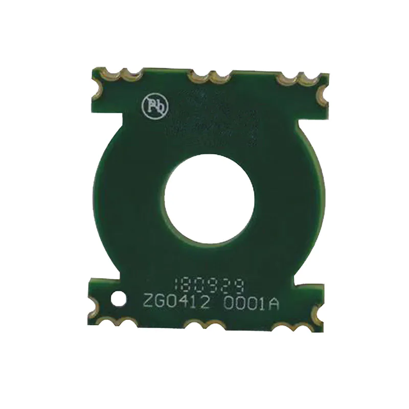


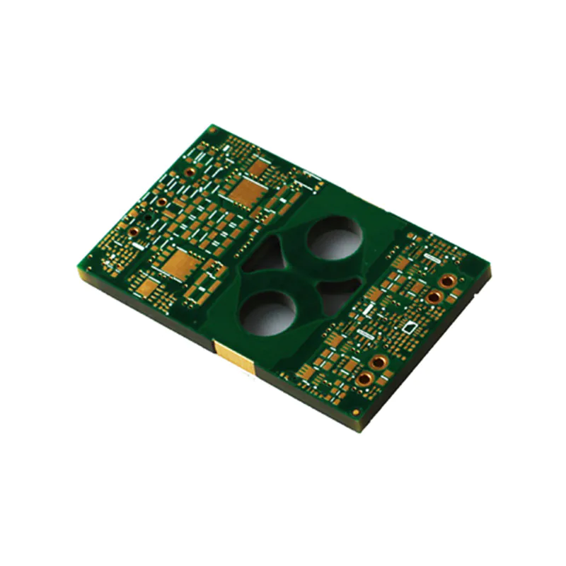
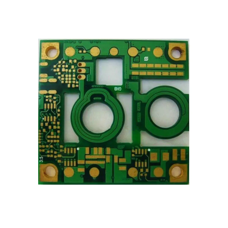
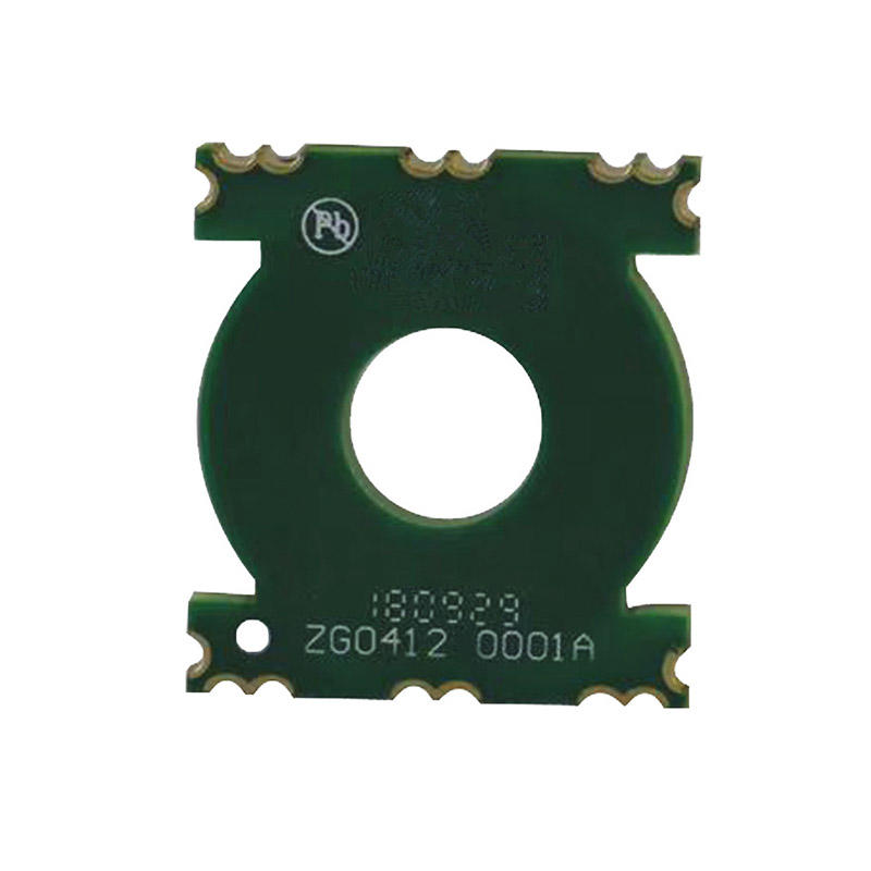
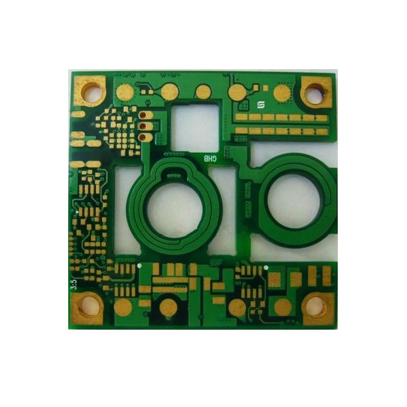
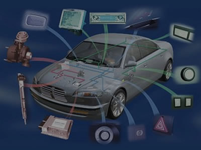
Thick copper board, refers to the circuit board whose inner layer base copper or outer layer finished copper thickness ≥2oz. Used to carry large current, reduce thermal strain and heat dissipation, mostly used in communications equipment, aerospace, automotive, network energy, planar transformers and power modules, etc.
With the more and more integrated chip technology, the circuit board is also constantly moving towards a light, thin, short, small direction, etching line width is getting smaller, but the current on the line needs to be carried more and more large.Therefore, the requirement for copper thickness is also increased to 102.9μm (3oz), 137.2m (4oz), even 171.5um (5oz), 205.7μm (6oz)
In the etching process, fresh etching solution is difficult to enter due to the thick copper; the pool effect is obvious.Then due to its own equipment capacity (etching process capacity) limitations, thick copper etching is often a difficult process.There are many factors affecting etching, Rocket PCB through many years of experience in the manufacture of thick copper, for different copper thickness, different lines of design, different etching methods, Here are some of our experiences.
1, When the thick copper board is etched, a more uniform etching line (linear) and etching factor can be obtained by alternating etching without changing the production conditions
2, Multiple etching is equivalent to an increased etching capacity, that is, a line that can be etched to a smaller spacing relative to a single etching.
3, When the thick copper is etched, the direction of the dense line length is used as the etching direction, and better etching factors and lines (linear) can be obtained.
4. Etching factor = etching line thickness/[downline width-online width)/2]; It has reference value as etching quality standard when thick copper etching.
> Our factory has invested in importing a large number of advanced production facilities such as Burkle laminator, Mitsubishi laser drill, Hitachi mechanical drill, Japan screen automatic exposure machine, LDI, AOI etc, realizing highly automated integrated manufacturing. With a monthly output of up to 250,000 square meters.
> Our suppliers have formed a complete production process, which is becoming more specialized, modern and large-scale, has signed long-term strategic cooperation agreements with well-known enterprises at home and abroad.
> Our superb quality and leading market position are guaranteed under the ISO9001, ISO14001, ISO/TS16949, OHSAS18001, ISO/IEC27001, UL, SGS, ROHS system with our strong technical development drive. We also insist on adopting 5S methods, Lean and Six Sigma quality systems.
> We provide real-time and in-depth technical support. Customized PCB application solutions, such as high speed, large capacity, high frequency, mixed pressure (hybrid structure), heat dissipation metal base solutions.
> Free DRC and DFM
> Rapid feedback on the layout, build-up, panels, impedance, material selection, design rules, manufacturability, costs of different solutions, use of micro vias, gold plating, special laminates and other engineering questions. When providing innovative solutions for our customers'products, we always consider maximizing the benefits for our customers.
> Rocket provides industry-leading support to our customers,we are more willing to help customers grow with us.
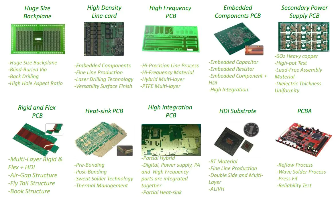
Advanced Product and Advanced Technology
> 24 hours online tech support and fast quote in 2 hours for standard board.
> Multiple different production lines meet the request of fast turn around of small batches and various PCB prototypes and mass production.
> Expedited production line for prototyping double-sided PCB up to 24 hours, 4 layers 48 hours, 6 layers 72 hours etc.
> Mass production of double-sided PCB 5-6 days lead time, multi-layer PCB 7-9 days.
> DHL, Fedex, TNT, UPS Express delivery, fully meet the customer's time requirements, on time delivery more than 99%


Security Industry
Quick Links
About Us
Contact Us
Tel:(+86) 158 9965 5195
Office:(+86) 755 23040566
E-mail:sales@sllpcb.com
Microsoft Teams:hank_168
WhatsApp:+86 186 0723 3179
Office Address:2207,Bid 4,He Gu Shan Hui Cheng,35#,Guang Tian Ro Yanluo street, Song Gang Town,518105 SHENZHEN, CHINA
Plant ADD: No 69, Lianfeng North Road, Xianxi Area, ChangAn Town, Dongguan, China.


