English


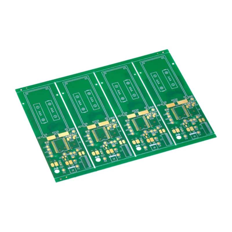
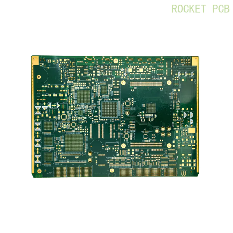
Double sided Fast PCB PCB prototyping quick turn around PCB production

Two-sided
PCB model, the foremost normally surface treatment is HASL. At constant
time, OSP, gold plating, immersion gold, immersion silver, is equally
applicable.
HASL- sensible appearance, simple to weld tin on the pad, easy welding, low price.
ENIG- stable quality, sometimes employed in the case of boding IC.
For
two sided board, using through hole within the middle connects
two-sided traces, and there are 2 more processes than single aspect
board, that is Electroless Copper and plating.
Double sided boards are wide used and relatively easy, each manufacturer can do, that the competition is usually on the price.
Some
makers use low grade CCL, soldermask ink is also comparatively low
cost, even the surface plating is skinny, leading to price variations.
At
Rocket PCB, we have been using top-grade materials, never cut corners,
quality is first-class, our strategy is tiny profits but fast turnover,
therefore within the premise of quality assurance, our PCB price is
extremely competitive, you're welcome to inquiry
here to get quick quotation!
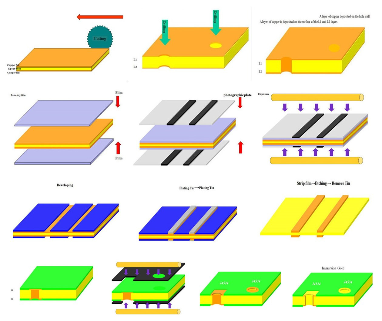
Customer requirements → engineering design materials → production work order MI→material cutting→baking board → drilling → electroless plating copper(PTH) →copper surface plating→ grinding Brush→ pattern exposure → develop→plating copper and tin →strip film→ etching → strip tin →soldermask→Immersion Gold→Routing→ET→HASL→FQC→warehouse
1, Cutting Material: Cut out easy-to-process dimensions from the whole sheet of copper clad laminate (CCL) with a certain thickness and foil thickness
2, Drilling: Drilling a conductive hole or plug-in hole on the board according to the computer drilling program
3,
PTH: A thin layer of chemical copper is deposited in the drilled hole,
with the aim of sinking a layer of copper through chemical methods in
non-conductive epoxy glass cloth substrates (or other substrates),
making it easy for the rear plating guide to form the circuit pattern;
4,
Full Plate Copper Plating: The main purpose is to protect the thin
layer of chemical copper from oxidation in the air, forming no copper or
holes in the holes.
5, Circuits (graphics transfer) is pasted with dry film on board. After exposure and development, circuit graphics are made.
6,
Pattern plating: Wire copper thickening plating on pattern circuit, so
that the hole and pattern copper thickness reached a certain thickness,
can load a certain amount of current
7,
Etching: Fade The graphics ink or dry film, etching off the excess
copper foil to obtain conductive line graphics. Remove the pattern ink
or dry film, etch out the excess copper foil to get the conductive
graphics
8, Remove tin: The tin layer on the formed graph is removed to reveal the required pattern
9,
Silk screen soldermask or paste soldermask dry film: Printing a layer
of soldermask ink on the board, or affixed with a layer of soldermask
dry film, after exposure, development to form soldermask layer, the main
purpose is to prevent short circuit between the lines at the time of
soldering
10, Immersion Gold/HASL:
Immersion gold or spray a layer of tin on the board where it needs to be
welded, making it easy to solder, while also preventing oxidation of
the copper surface at the place
11, Silkscreen: printing some iconic words on the board, mainly convenient for customers to install components
12, Routing: Process the profile of the Board
13, Electrical test: Detecting whether there is an open short circuit in the PCB by means of a closed loop
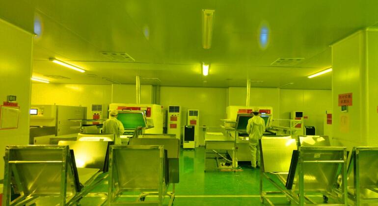
Strong production strength, can meet the batch needs of different customers
> Well-known cooperative suppliers import advanced equipment and production technology from Germany, Japan, Taiwan and other regions, with a monthly output of up to 250,000 square meters.
> For a long time our suppliers have formed a complete production process, which is becoming more specialized, modern and large-scale.
> We passed ISO 9001 quality system, TS16949, UL standard, ROHS standard and SGS lead-free certification and related industry certification.
> Senior R &D team, tailor-made application solutions, like high speed, high capacity and high frequency, press-fit, heat-sink solutions
> In general, customers provide gerber files and Rocket senior R&D engineers team audit and optimize them free of charge (Free DRC and DFM)
> For customers with special requirements, we can provide personalized solutions, design drawings, develop new products, and provide relevant technical support according to their needs and combined with our practical experience.
Service Advantages
> Multiple production lines meet the requirements of mass production and quick turnover of small batches and prototype
> Expedited production line for prototyping double-sided up to 24 hours, 4 layers 48 hours, 6 layers 72 hours etc.
> Mass production of double-sided board 5-6 days lead time, multi-layer board 7-9 days.
> DHL, Fedex, TNT,UPS Express Direct, fully meet the customer's time requirements.
> Strict production and testing, 100% outgoing pass rate
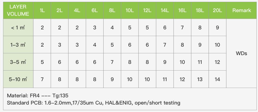
> Provide 1-64 layers of different thickness, different materials, different processes of product customization, of which the CCL using A-class raw materials, high quality assurance;
> Advanced technology for rigid, rigid-flex, flexible, RF, metal core, backplane, ceramic, HDI and so on.
> Eight major surface treatment technology and high-quality ink printing, beautiful and reliable
> Dozens of tests such as open/short circuit testing, impedance testing, solderability testing, thermal shock testing, metallographic micro-slicing analysis, halogen-free testing, etc.Rocket PCB supply chain meticulously practices all-around quality management and actively introduces and implements multi-domain system management. We have successively obtained ISO9001, ISO14001, IATF16949, OHSAS18001, ISO/IEC27001, ISO13485 and AS9100 certifications.
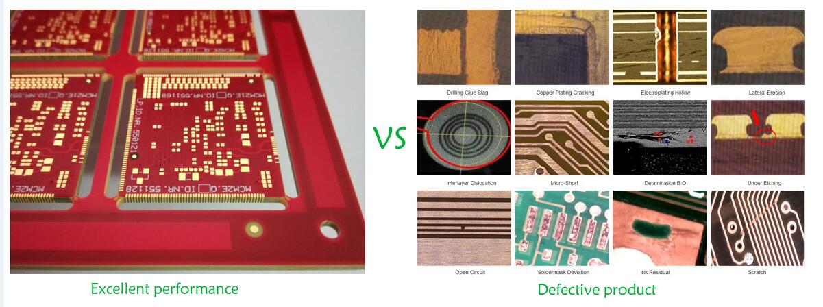
Due to the circuit board industry manufacturing level is uneven, if accidentally selected to the low-end manufacturing plant, there will be poor engineering data processing, old equipment, management confusion, poor parameter control, improper operation of personnel and other process issues, such as the following quality defects.


Product Message
QUICK LINKS
CONTACT US
Office: (+86) 755 23040566
Tel: (+86) 158 9965 5195
E-mail: sales@rocket-pcb.com
Skype: Hans@Rocket-PCB
Whatsapp: 86 1589965 5195
Office Address: 301 Building/B, Huafeng Digital Technology Industrial Park, Chaoyang Ro, Yanchuan, Songgang,518105 Shenzhen, China.
Plant ADD.: No 69, Lianfeng North Road, Xianxi Area, ChangAn Town, Dongguan, China.