


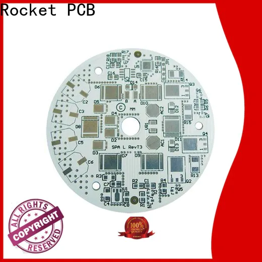
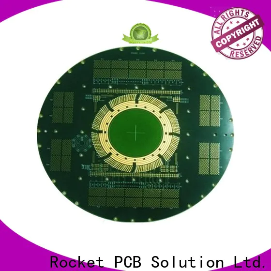
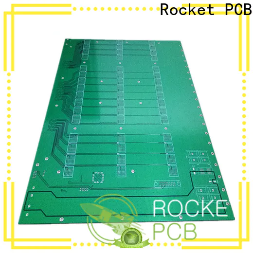
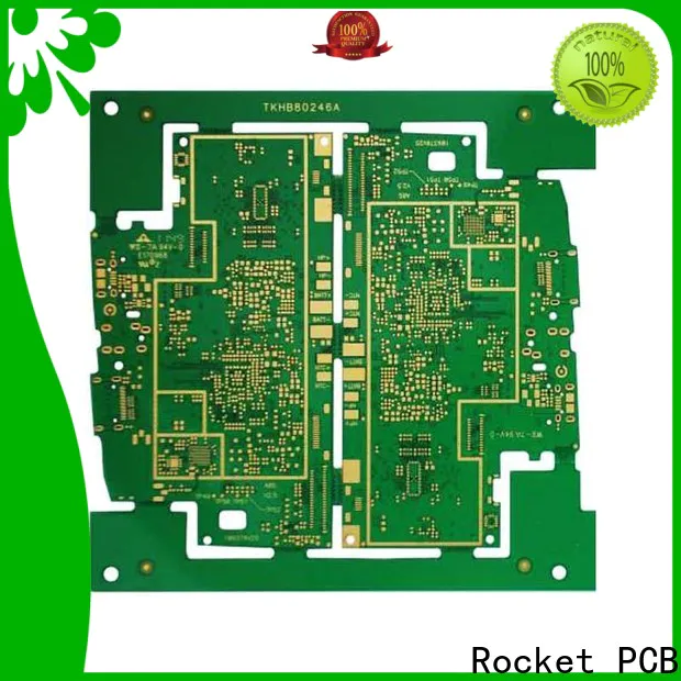
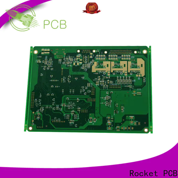
一、Basic Principles of PCB Lamination ProcessThe basic principle of PCB lamination is to bond and cure multiple layers of board materials through heating and pressure, so as to form an integrated multi-layer PCB. In this process, precise control of temperature and pressure is critical. Meanwhile, multiple factors such as material expansion, contraction and stress release need to be taken into account.The core of the lamination process lies in the application of prepreg (PP). As a sheet-shaped bonding material composed of resin and glass fiber, prepreg mostly adopts thermosetting polymers such as epoxy resin. Under heated and pressurized conditions, the resin softens and flows to fill the gaps between layers and form a uniform bonding layer. Meanwhile, the macromolecular chains of the resin diffuse and penetrate mutually under temperature and pressure, forming stable chemical bonds and realizing the integral bonding of multi-layer PCBs.二、Technological Process of PCB LaminationThe technological process of PCB lamination consists of multiple key steps, each exerting a vital influence on the quality of finished products.1. Preparatory WorkAs the initial stage of lamination, this procedure mainly covers material preparation and cleaning. Required materials include copper clad laminates, prepregs, kraft paper cushions and so on. All materials must be kept dust-free and spotless to guarantee lamination quality. In addition, steel plates need thorough cleaning to remove surface glue stains and slight scratches, laying a solid foundation for subsequent lamination operations.2. Board Placing and AlignmentThis process refers to accurately aligning multi-layer boards in accordance with design specifications. Extremely high precision is required here, since even minor misalignment may lead to interlayer sliding or poor circuit connection in subsequent processing. Positioning pins and other tools are adopted to ensure precise lamination alignment.3. Pre-laminationAlso known as pre-stacking, it is the preliminary bonding process implemented at low temperature and low pressure. Its core purpose is to achieve initial combination of interlayer materials and get ready for formal lamination. Preheating and low pressure are applied to avoid excessive flow of interlayer materials and prevent air and impurities from being trapped inside. It effectively cuts adjustment errors and boosts production efficiency in formal lamination.4. Formal LaminationIt is the core procedure carried out under high temperature and high pressure. During this stage, interlayer materials fully flow and cure to form rigid integrated multi-layer PCBs. Accurate temperature and pressure control is essential to realize complete bonding of all layers and stable electrical performance. Resin flows sufficiently to fill interlayer gaps and form uniform adhesive layers. Meanwhile, macromolecular chains inside the resin diffuse and interpenetrate to form firm chemical bonds.5. Cooling and DemouldingCooling treatment is conducted right after lamination. Demoulding is carried out when the temperature drops to a specified value to obtain finished multi-layer PCBs. Resin gradually cures and forms stable chemical bonds during cooling. Careful operation is required in demoulding to prevent damage to the boards.6. Post-treatmentIt includes removing excess substances, edge trimming and surface finishing. Excess resin and residual kraft paper generated during lamination are cleaned away first. Board edges are trimmed neatly by routing machines or milling machines. Surface treatments such as electroplating and tin spraying are implemented as required to enhance conductivity and solderability of PCBs.三、Key Control Factors of PCB LaminationSpecial attention shall be paid to multiple core control factors in PCB lamination to ensure qualified lamination quality and high production efficiency.1. Temperature ControlTemperature dominates resin fluidity and curing progress. Different types of resin require matched lamination temperature and holding time. Insufficient temperature causes inadequate resin flow and incomplete gap filling; excessive temperature leads to excessive resin flow, resulting in board deformation or interlayer short circuits. Precise temperature regulation is necessary to meet standard resin fluidity and curing requirements.2. Pressure ControlSuitable pressure ensures tight material bonding, while excessive pressure will cause board deformation. Even pressure distribution is indispensable to avoid defective lamination. Pressure value shall be adjusted according to board layers and thickness to achieve tight interlayer adhesion. Uniform pressure distribution must be guaranteed to prevent local deformation and interlayer separation.3. Time ControlLamination duration directly determines curing effect. PCBs with different materials and structures need different lamination time. Insufficient time results in incomplete resin curing and weak mechanical and electrical properties; excessive time causes over-curing, leading to board brittleness and cracking. Accurate time control ensures ideal curing effect.4. Material SelectionVarious materials differ greatly in expansion and shrinkage coefficients, so proper material selection is the premise of successful lamination. Practical service environment, performance requirements and production costs shall be taken into full consideration. Material compatibility and matching performance also need verification to realize stable structural bonding.5. Environment ControlAmbient conditions greatly affect final lamination quality. Excessive humidity makes resin absorb moisture and weaken curing effect; poor cleanliness causes surface contamination and damages electrical stability. Strict control over ambient humidity and cleanliness is mandatory in production.四、Challenges and Solutions of PCB LaminationWith the continuous upgrading of electronic products, PCB lamination technology is facing increasingly severe challenges, mainly including growing complexity of multi-layer boards, inconsistent material compatibility, higher equipment precision standards and process parameter optimization demands.1. Increased Complexity of Multi-layer BoardsDiversified functions of electronic products keep increasing PCB layers, which greatly raises lamination difficulty. Higher standards are set for alignment accuracy and lamination uniformity. The solution is to deploy high-precision positioning and lamination equipment to realize accurate alignment and uniform adhesive layer formation.2. Inconsistent Material CompatibilityMaterials from different manufacturers have distinct physical and chemical properties, which requires continuous compatibility tests and process debugging. Manufacturers shall strengthen communication and cooperation with material suppliers to master material characteristics timely and optimize process parameters dynamically.3. Higher Requirements for Equipment PrecisionHigh-precision equipment involves high investment cost, yet it is vital to improve lamination quality and production efficiency. Enterprises need to increase investment and R&D input in high-end precision equipment, and strengthen daily maintenance to ensure long-term stable operation.4. Optimization of Process ParametersParameter optimization is the core approach to improve lamination quality and production efficiency. Process parameters shall be adjusted flexibly according to product types and production batches to stabilize product quality. Adjusting temperature, pressure and holding time can optimize resin flow and curing state; optimizing layout and board placement methods can promote alignment accuracy and lamination uniformity.五、Summary and ProspectAs an indispensable core procedure in PCB manufacturing, lamination quality and efficiency directly decide the reliability and overall performance of electronic products. In-depth mastery of lamination principles, technological flows and key control factors contributes to process optimization and quality improvement. Nevertheless, the rapid iteration of electronic products brings new difficulties to lamination technology.In the future, driven by technological innovation, PCB lamination technology will achieve continuous upgrading and improvement. Sustained technical research and process upgrading will help PCB manufacturers gain competitive advantages, satisfy high-end market demands and boost the innovation and development of electronic industry. Meanwhile, greater importance shall be attached to environmental protection and sustainable development, promoting PCB lamination technology toward greener and more efficient development direction.In conclusion, PCB lamination is a sophisticated and refined manufacturing process requiring constant exploration and optimization in practical production. With joint efforts of all industry practitioners, PCB lamination technology will embrace broader development prospects.
Read More>>
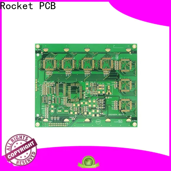
All Products
-
Best PRODUCTS Manufacturer
-
Certificated Hybrid PCB Wholesale
-
Wire Bonding PCB Bulk
-
Top Thermal Management PCB
-
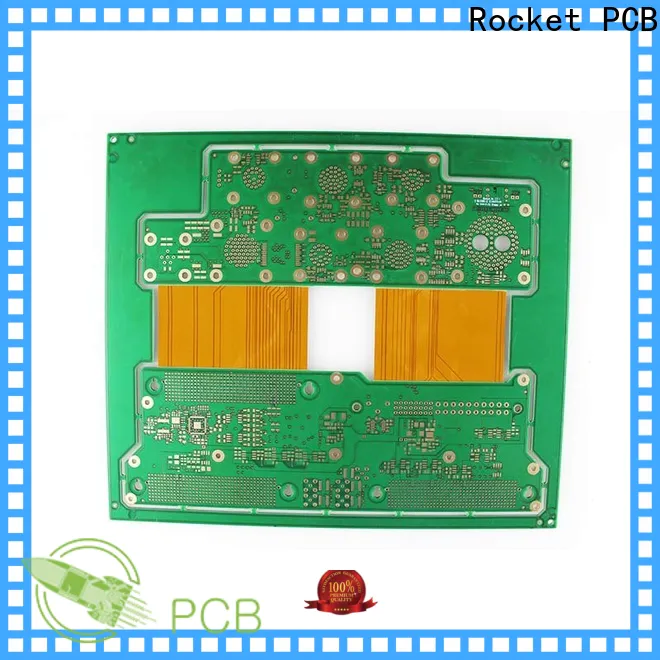
Quality Rigid-flex PCB Wholesale
-
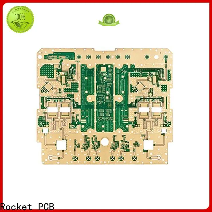
Customized RF&Microwave PCB
-
Top Multilayer PCB Warranty
-
Quality Aluminum PCB
-
Top Large PCB Bulk
-
Quality IC Substrate PCB Wholesale
-
Certificated Heavy Copper PCB
-
Top HDI PCB
-
Gold Finger PCB Supplier
-
Hot Flex PCB
-
Best Embedded PCB
-
Single&Double Sided PCB Factory
-
Top Ceramic PCB
-
Cavity PCB For sell
-
Hot Backplane PCB For sell
-
Any-layer PCB Factory
-
Certificated Hybrid PCB Wholesale
Relevant Articles
In-Depth Analysis of the PCB Lamination Process
Top 50 PCB Manufacturers in China (2025)
Top 50 PCB Companies in China (2025)China PCB Industry Trends in 20251.AI Servers Are Driving Demand for High-End PCBsAI computing infrastructure has become one of the fastest-growing segments in the PCB industry.The rapid deployment of GPU servers, AI accelerators, 800G switches, and high-speed optical modules is significantly increasing demand for:High-layer-count PCBsHigh-speed backplanesLow-loss materialsHigh-frequency PCB designsLeading Chinese PCB companies such as Shennan Circuits, WUS, Victory Giant, and Shengyi Electronics are benefiting from the global AI boom.2. Automotive Electronics Continue to ExpandElectric vehicles require far more PCBs than traditional fuel vehicles.PCBs are widely used in:Battery Management Systems (BMS)Autonomous driving systemsDomain controllersIntelligent cockpitsPower electronicsRadar and sensorsCompanies including Kinwong, Avary Holding, Dongshan Precision, and Suntak Technology are actively expanding automotive PCB production capacity.3. High-Frequency and High-Speed Materials Are Growing RapidlyThe development of 5G, AI, cloud computing, and advanced networking equipment continues to accelerate demand for high-performance PCB materials.Chinese material suppliers such as Shengyi Technology and Huazheng New Material are pushing domestic substitution in high-end PCB laminates.4. IC Substrate Localization Is AcceleratingIC substrates remain one of the most critical high-end PCB segments.Chinese companies are increasing investment in:ABF substratesAdvanced packaging substratesSemiconductor packaging materialsFastprint, Shennan Circuits, and Unimicron are among the major players expanding in this sector.5. Smart Manufacturing Is Becoming the Industry StandardMore PCB factories are adopting:Automated production linesAOI inspection systemsMES manufacturing systemsAI-powered quality inspectionDigital factory managementThe future of PCB manufacturing is moving toward intelligent and highly automated “lights-out factories.”Leading PCB Companies in ChinaShennan Circuits (SCC)Shennan Circuits is one of China’s leading high-end PCB manufacturers.The company has strong capabilities in:Communication PCBsSemiconductor substratesElectronic assemblyHigh-speed server PCBsAerospace electronicsIts products are widely used in AI servers, telecom infrastructure, automotive electronics, and data centers.Avary HoldingAvary Holding is one of the world’s largest PCB manufacturers and a major supplier in the Apple supply chain.Its core products include:Flexible Printed Circuits (FPC)HDI boardsSmartphone motherboardsConsumer electronics PCBsThe company is also expanding into automotive and AI-related applications.WUS Printed CircuitWUS is highly competitive in high-speed communication PCBs and server PCBs.With the explosive growth of AI infrastructure, the company has seen strong demand in:800G switchesData center PCBsHigh-speed backplanesCloud computing hardwareVictory Giant TechnologyVictory Giant Technology has experienced rapid growth in recent years.The company has become increasingly competitive in:GPU graphics card PCBsAI server PCBsHigh-layer-count PCBsAutomotive electronicsIt is now considered one of China’s key high-end PCB manufacturers.China PCB Industry Supply ChainUpstream MaterialsThe upstream PCB supply chain mainly includes:Copper clad laminates (CCL)Copper foilGlass fiber clothEpoxy resinSolder mask inkDry film materialsMajor suppliers include:Shengyi TechnologyHuazheng New MaterialHongchang ElectronicsNord Copper FoilTongling Copper FoilMidstream PCB ManufacturingPCB manufacturing mainly covers:Single-sided PCBsDouble-sided PCBsMultilayer PCBsHDI boardsFlexible PCBs (FPC)IC substratesDownstream ApplicationsPCBs are widely used in:AI serversAutomotive electronicsIndustrial automationTelecommunicationsConsumer electronicsMedical equipmentMilitary electronicsSemiconductor packagingFuture Outlook of China’s PCB IndustryOver the next few years, China’s PCB industry is expected to continue moving toward high-end manufacturing and advanced technology applications.The following areas are expected to become major growth opportunities:AI server PCBs800G networking PCBsAutomotive electronics PCBsIC substratesHigh-frequency high-speed materialsSemiconductor packagingSmart factoriesGreen manufacturingAs the global electronics industry continues to evolve, Chinese PCB manufacturers are gradually shifting from manufacturing advantages to technology-driven competitiveness.ConclusionIn 2025, China’s PCB industry is entering a new era of technological upgrading and industrial transformation.Leading companies such as Shennan Circuits, Avary Holding, WUS, Victory Giant, and Kinwong are driving the industry toward higher-end applications, intelligent manufacturing, and global expansion.With continued growth in AI, electric vehicles, cloud computing, and semiconductor industries, China’s PCB sector is expected to play an even more important role in the global electronics supply chain.About Rocket PCBRocket PCB closely integrates manufacturing, logistics, and PCB supply chain management. This allows us to complete PCB design, assembly, and product distribution faster and at lower cost while maintaining consistent product quality.We always put our customers’ interests first and are committed to providing innovative solutions for electronic product manufacturing.We welcome all types of PCB orders and are ready to support your projects with professional service and reliable manufacturing capabilities.Contact us: sales@rocket-pcb.com
Read More>>
Choosing the Right Materials for Your PCB Batch: A Comprehensive Guide
1. IntroductionSelecting suitable substrate materials stands as one of the most critical steps in PCB batch production. It directly affects electrical performance, thermal reliability, production yield and overall cost. For mass manufacturing, consistent material performance across different batches is particularly vital, so standardized and reasonable PCB material selection becomes essential.2. The Role of PCB SubstratesA typical PCB substrate consists of core laminate, prepreg and copper foil. In batch production, stable resin content, glass fabric structure and dielectric thickness are required to ensure consistent impedance, reliable lamination and unified board quality. As a cost-effective and process-friendly option, FR-4 is the most widely used general-purpose substrate in the industry.3. Key Performance Parameters of PCB MaterialsDielectric Constant (Dk)It affects signal propagation speed and impedance stability. High-speed circuits prefer low-Dk materials to reduce signal delay.Dissipation Factor (Df / Loss Tangent)It indicates high-frequency signal loss. Materials with lower Df deliver better signal integrity for RF and high-speed transmission designs.Glass Transition Temperature (Tg)It represents the material’s heat resistance during reflow soldering and long-term operation, effectively preventing board warpage and delamination.Coefficient of Thermal Expansion (CTE)Matching the CTE of substrate and copper foil can avoid thermal stress problems such as via cracking and layer separation.4. Common PCB Substrate Types & Application ScenariosStandard FR-4Cost-effective and easy to process, ideal for conventional circuits below 1GHz.High-Frequency Low-Loss MaterialsWith stable low Dk and Df values, suitable for 5G, RF and high-speed digital products, though at a higher cost.High-Tg Epoxy MaterialsExcellent heat resistance and anti-warpage capability, perfect for multi-layer thick boards and heavy copper PCBs.Polyimide MaterialsCapable of adapting to extreme temperatures from -200°C to 260°C, widely used in aerospace, military and downhole sensor devices.5. Material Selection Guidelines for Batch ProductionUse standard FR-4 for scenarios below 1GHz; adopt professional high-frequency substrates for applications above 1GHz.Follow IPC-4101 and IPC-6012E industry standards, and choose suppliers with stable batch traceability.Adopt hybrid stack-up design (FR-4 core board combined with low-loss outer layers) to balance performance and cost for high-speed projects.6. Common Design & Manufacturing PitfallsInsufficient moisture resistance of materials easily causes delamination during reflow soldering.Asymmetric stack structure will lead to serious PCB warpage.Unstable dielectric thickness results in impedance deviation and degraded signal integrity.7. ConclusionPCB material selection needs to comprehensively balance electrical properties, thermal performance, mechanical characteristics and cost. Standard FR-4 can meet most conventional design needs, while high-speed, RF and harsh environment scenarios require dedicated high-frequency or special substrates. Abiding by industry specifications and controlling batch consistency helps manufacturers achieve stable yield, reliable performance and cost optimization in PCB mass production.
Read More>>


