
Hot products
English


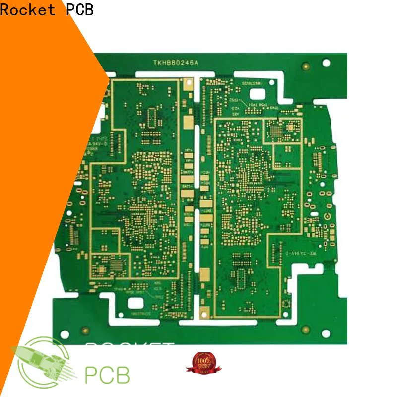

As one of the most popular products in Rocket PCB Solution Ltd, HDI PCB wins increasing popularity.
FR4
is an essential material for manufacturing the product. Various brands
and sizes are available. It is designed to meet the industry criterion.
Key technologies used in production include LDI, Laser etching.
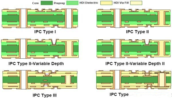
Supported by 4+N+4 structure capability, HDI PCB is of such
characteristics as improves the wiring density of the inner signal
layer,great help to Power integrity ang singal integrity. HDI PCB is
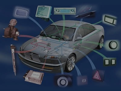
practical for communication, medical, military, security, industrial,
automotive fields.
Guided by the principle of 'Service
creates value, service wins respect and service builds brand ', we
continue to grow and develop. Welcome people from all walks of life to
consult and cooperate. https://www.rocket-pcb.com
Rocket PCB Solution Ltd is passionate about making a difference in the manufacturing industry, so we’re always expanding the research and driving the innovation to find new and practical solutions.
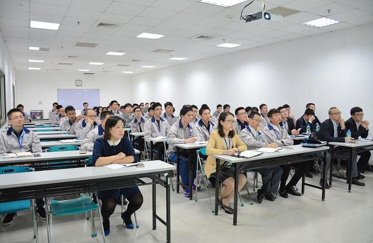
Throughout years of hard work in the manufacturing industry, the R&D team has served as a pillar of Rocket PCB. As time goes by, the R&D team has been expanded to 50 people. With the accumulation of 10 years of experience, each member is skilled at dealing with engineering data by absorbing in advanced technology. All of them are able to provide technical service for customers.
HDI PCB
HDI PCB is one of the most distinguished product among those collections in Rocket PCB Solution Ltd.
It comes with various structures. The design of it caters to varied needs of customers at home and abroad. Impedance control, dense circuit is adopted to produce high-quality HDI PCB. With such parameters as 4+N+4 sturcture, high reliable characterize HDI PCB.
ROCKET PCB SUMMARY
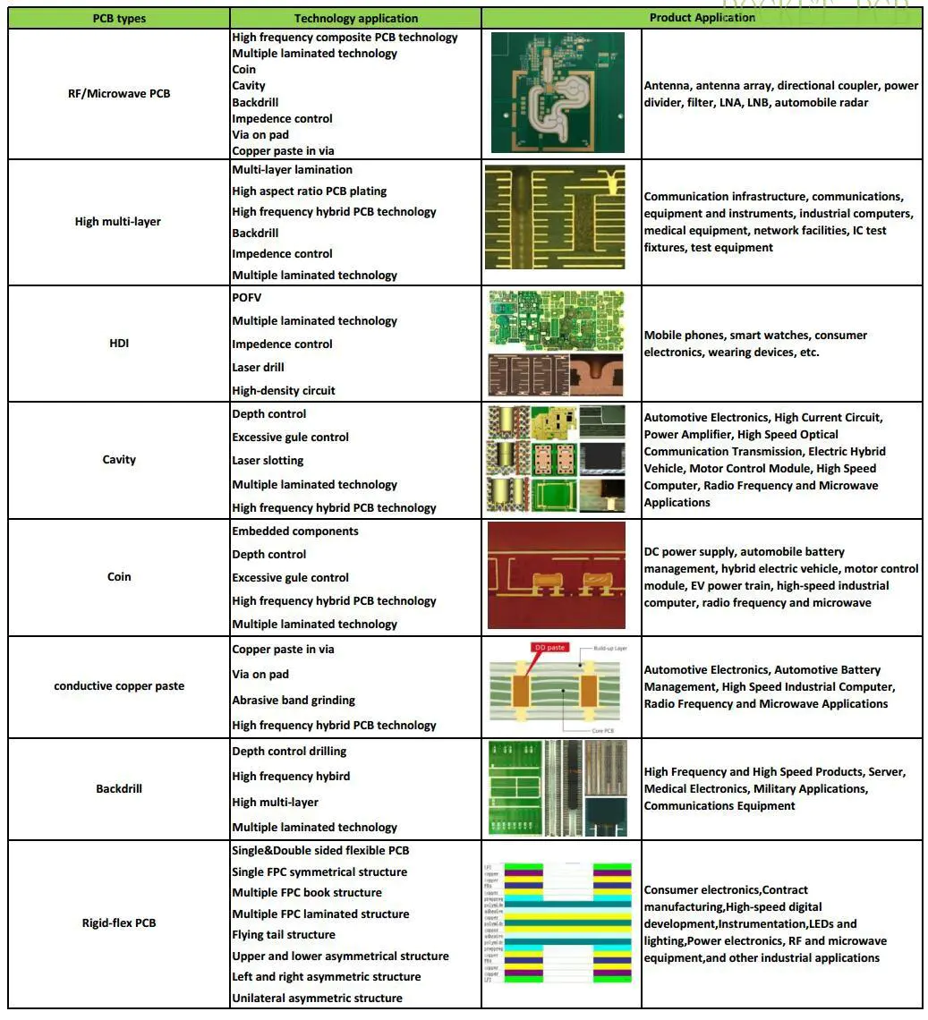
Rocket PCB is an innovative manufacturer focusing on electronic manufacturing. Rocket PCB is dedicated to spending 10 years of efforts advancing itself. We develop, produce and sell numerous successful high-quality products, including rigid, rigid-flex, HDI, any layer, Flex, large-size, embedded, RF, LED, backplane, metal substrate, ceramic substrate, IC structure, high-frequency, heavy copper. High quality and high reliability.

SPECIALIZED MANUFACTURING
Conductive materials and core-to-core bonding
Embedded components
RF connector attachment
Laser direct imaging (LDI)
Laser etching
Laser forming
Multi-level cavity construction
Plated cavities and edges
Composite/hybrid Structures
N+N dual press-fit
Dual-drill
Bonding on metal core
Bulid-up HDI
Long-short and staged gold finger
A wide range of professional manufacturing solutions, can be used for thermal energy (CTE) structural coefficients, thermal challenge design and application, extreme and unique HDI structures, and RF control
A wide range of professional manufacturing solutions, can be used for thermal energy (CTE) structural coefficients, thermal challenge design and application, extreme and unique HDI structures, and RF control
A wide range of professional manufacturing solutions, can be used for thermal energy (CTE) structural coefficients, thermal challenge design and application, extreme and unique HDI structures, and RF contro

CAPABILITIES
3mil line and space
4mil laser defined vias
6mil chip-on-board
6mil mechanically drilled vias
Conductive and non-conductive via fill
Dual backdrilling
Sequential lamination
Mixed dielectric
Heatsink Bonding
Heavy copper/thermal vias
Blind/buried vias
Stacked and staggerd microvias

Design Rules Check(DRC)
Electrical Testing
Automated Optical Inspection(AOI)
X-Ray
Plating thickness testing
Metalized vias inspection
Thermal shock testing
Surface peelability testing
Impedance control testing
100% visual inspection
Solderability testing
Ionic cleanliness testing
Metallographic microscopic analysis
High voltage testing
Insulating resistance testing

FEATURES
PTFE
High speed/low loss
High temperature
Low CTE
Lead-free, HASL, ENIG, EPENIG, Immersion Silver, Tin, Gold finger
Combination surface finished
Copper-filled microvias
Due to the circuit board industry manufacturing level is uneven, if accidentally selected to the low-end manufacturing plant, there will be poor engineering data processing, old equipment, management confusion, poor parameter control, improper operation of personnel and other process issues, such as the following quality defects.
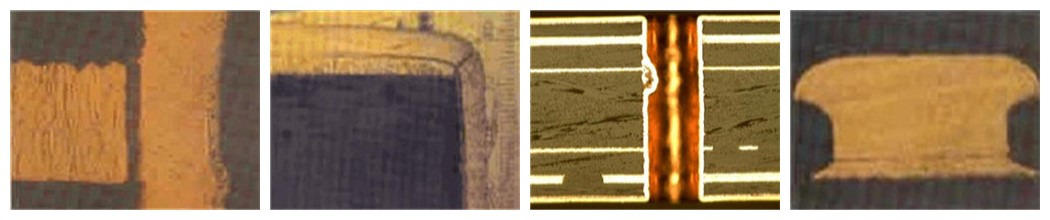
Drilling Glue Slag Copper Plating Cracking Electroplating Hollow Lateral Erosion
Interlayer Dislocation Micro-Short Delamination B.O. Under Etching
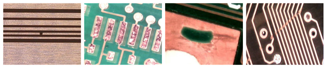
Open Circuit Soldermask Deviation Ink Residual Scratch
These problems will greatly increase the ratio of defective circuit boards, resulting in a sharp increase in the number of rework, insufficient delivery quantity, extended delivery and so on unexpected problems. Therefore, choosing a manufacturer that is highly reliable and of good quality is the perfect choice for you, the quality of the customer circuit board will be guaranteed from the source.
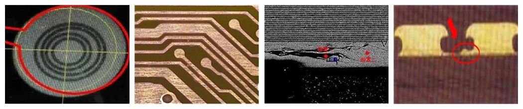
However, In Rocket, with advanced production equipment, excellent PCB solutions and complete testing methods, we have specialists working on their particular fields with the thorough mastery of their particular discipline in each of the production facilities. Training, as well as technical exchanges, are held frequently, tackling problems in key technologies and configuring scheme of equipment and allowing professionals to get up to speed on the essential tools that many organizations value today in the manufacturing industry. Thanks to those above, we have greatly improved the strength and won international reputation.


Quick Links
About Us
Contact Us
Tel:(+86) 158 9965 5195
Office:(+86) 755 23040566
E-mail:sales@sllpcb.com
Microsoft Teams:hank_168
WhatsApp:+86 186 0723 3179
Office Address:2207,Bid 4,He Gu Shan Hui Cheng,35#,Guang Tian Ro Yanluo street, Song Gang Town,518105 SHENZHEN, CHINA
Plant ADD: No 69, Lianfeng North Road, Xianxi Area, ChangAn Town, Dongguan, China.


