
English


Typical Index | Process Capability | Typical value |
Layers | 14L | 10L |
Size | 18.5”×24.5” | 18.5”×24.5” |
Total Thickness | 0.3mm≤T≤2.5mm | 0.8mm |
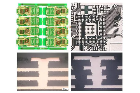
Min. L/S | 2.5mil/2.5mil | 2.5mil/2.5mil |
Blind via dia. | 3mil-5mil | 4mil |
Min. BGA Pitch | 0.4mm | 0.5mm |
Dimple | ≤15um | 15um |
Min. dielectric thk. For microvia | 2mil | 3mil |
HDI structure | 4+N+4 | 3+4+3 |
Soldering condition | LF Reflow 5X (260℃ peak ) | LF Reflow 5X (260℃ peak ) |
Application | Mobile, tablets, smart watch, etc. | |
HDI PCB refers to High Density Interconnect printed circuit board, also known as Build-up PCB. HDI PCB has finer lines and spacing, micro vias such as buried or blind vias, smaller capture pads and higher density of connection pads. Unlike traditional PCBs, HDI PCBs use laser drilling equipment to achieve the buried and build-up hole over-hole requirements. High density interconnect PCBs make the end product more efficient and allow for faster transfers.
Features
● Lighter weight
● Faster transfer speeds
● Reduced power usage
● Flexibility in component selection
In recent years, the most popular HDI in high-end smart phone is HDI in any layer, which requires blind hole connection between any adjacent layers. It can save nearly half the volume on the basis of ordinary HDI, thus freeing up more space to accommodate batteries and other components.
Any HDI layer needs advanced technologies such as laser drilling and electroplating plug. It is the HDI type with the most difficult production and the highest added value of products, which can best reflect the technical level of HDI. At present, due to the strong technical and financial barriers, the production capacity is mainly concentrated in Japan, Korea, Taiwan and Austria AT&S and other factories. The domestic start is relatively late, and there are few PCB manufacturers with capacity for mass production.
Rocket PCB company's technological process continues to improve, high multi-layer board, HDI technology ranks the forefront in China. The company has strong technical strength, strong technology research and development ability and complete process chain, complete PCB production line, large product span, production capacity covering HDI board, any layer interconnection HDI, high density multi-layer board and fast PCB prototype business.
As the earliest PCB manufacturer to realize HDI mass production in China, the technology process continues to improve.
High Multi-Any layers High Speed printed circuit board
QUICK LINKS
CONTACT US
Office: (+86) 755 23040566
Tel: (+86) 158 9965 5195
E-mail: sales@rocket-pcb.com
Skype: Hans@Rocket-PCB
Whatsapp: 86 1589965 5195
Office Address: 301 Building/B, Huafeng Digital Technology Industrial Park, Chaoyang Ro, Yanchuan, Songgang,518105 Shenzhen, China.
Plant ADD.: No 69, Lianfeng North Road, Xianxi Area, ChangAn Town, Dongguan, China.


